

The need for bottom-side AOI came at the same time that selective soldering became more popular. A majority of the components placed on a circuit board are applied using surface mount technology. However, in the automotive industry, the circuit boards contain more through-hole parts that need soldering. Automated selective soldering equipment became popular to solder the through-hole parts on the bottom-side of the board. Bottom-side inspection was also needed after dipping and wave soldering.
Bottom-side inspection
Historically, through-hole inspection was done manually by an operator or semi-automated, often using 2D bench top systems where the PCB was inserted by hand. There was little standardization in the electronics assembly industry so there were considerable variations from process to process and customer to customer. Standardizing the inspection operation and specifications was difficult. Because the process was operator-dependent, it not only lacked accuracy and consistency, it could also result in contamination and mishandled boards. Another drawback was that the inspection process was slow. Without automation, how could the inspection process be viable?
2D and 3D automated optical inspection of the top side of a PCBA has been around for a long time. In an effort to inspect the bottom-side, some companies manually flipped the board and then placed the boards into an AOI system. While this was a way to provide quality inspection of the bottom side, once again handling and contamination problems arose. Some companies added flippers to the line, but the added step of flipping decreased throughput.
Solution for market demand
Although Saki has had equipment to inspect both sides of a circuit board since 2015, the systems weren’t designed to handle today’s larger boards and taller components. As more customers started to request a bottom-side inspection system that could accommodate these new conditions, the company looked at ways to adapt its proven 2D line-scan technology and latest AOI systems to a 2D bottom-side AOI inspection system that could solve their inspection requirements.
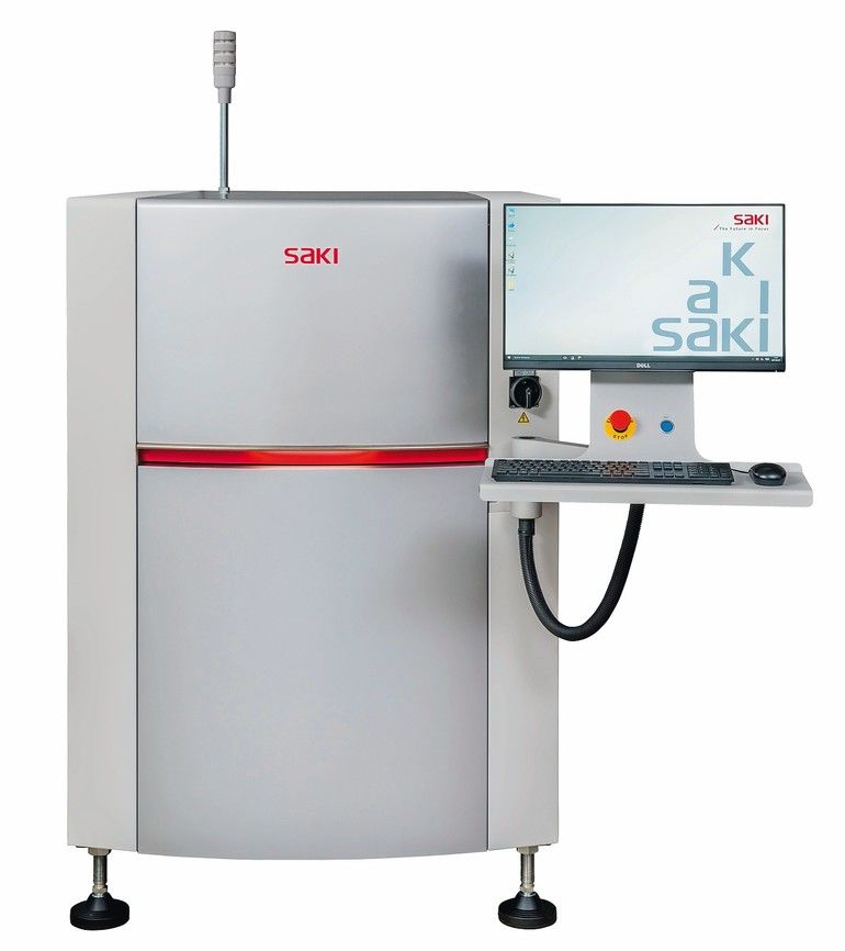
The result was the 2Di-LU1 2D automated bottom-side inspection system. It accommodates L-size 500 x 460 mm and 610 x 610 mm frames and handles tall components with clearances of 130 mm on the top side and 40 mm on the bottom. There are two different handling systems, a standard conveyor belt and a chain, and it’s equipped with space for return conveyor availability on the bottom side of the machine. The machine can carry up to 12 kg of PCB weight, which is suitable for a soldering jig frame operation.
Easy software configuration
The 2Di-LU1 software includes the company’s proprietary Fujiyama algorithm, which provides complete through-hole joint inspection in a single step. It simultaneously inspects for copper exposure, pin detection, pin-holes, solder fillet abnormalities, missing components, soldering problems, and bridges. Inspection is not only performed for through-holes; a complete AOI inspection is done for parameters, such as polarity. Extra Component Detection (ECD) inspects for scratches, contamination, solder balls, and other foreign objects during the through-hole device inspection process. The programming is very easy — just specify the area of interest and target size. Auto tuning, which optimizes inspection parameters automatically based on an SPC approach, is also available. ECD has been used in the automotive industry for several years and complies with the IPC-A-610 standard.
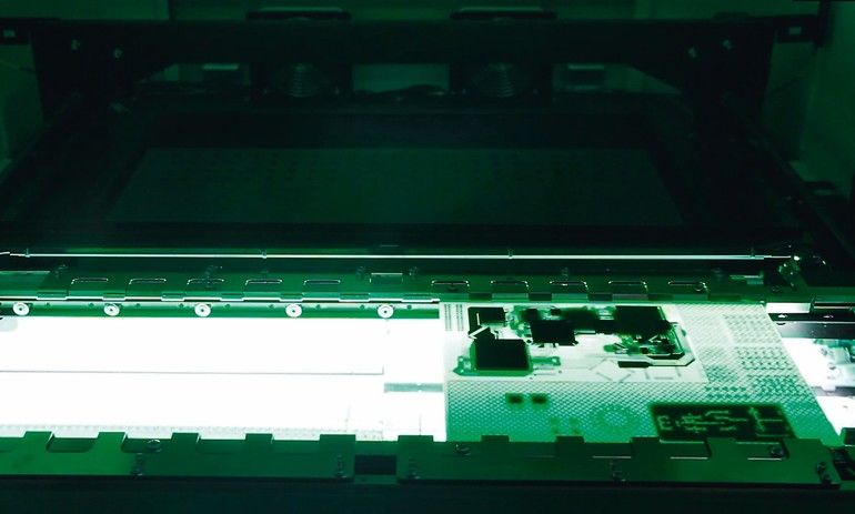
Saki invented 2D line-scan technology in 1994 and has continued to perfect it. It can scan a circuit board in one pass, capturing an entire 400 mm x 400 mm board’s field of view in less than 8 seconds, making it a fast through-hole inspection system. This speed is critical for takt time in the wave soldering process. By eliminating the loading and unloading process for flipping, it can keep up with the line speed needed in the automotive industry and increase throughput.
Having an automated inline system saves the cost of using an operator and reduces time and floorspace. As with all Saki inspection systems, the platform starts with a solid base and stable construction, so the platform can withstand vibrations, while axes stay aligned during operation. Also, images are clear, there is greater noise resistance, and the data secured by the system remains accurate. There is less hardware, so diagnostics are simple, and the cost of the hardware is lower.
The camera system gives excellent image contrast, quality, and a clear image. Coaxial top lighting reduces shadowing for effective solder joint inspection. Since the through-hole inspection algorithm uses gray scale analysis for solder inspection, the coaxial top lighting provides better contrast on the soldering fillet, which extends the inspection capability of the through-hole solder joint.
The software is integrated to function similarly to the company’s other AOI and solder paste inspection (SPI) systems, with the same easy and simple GUI. The solder meniscus is evaluated based on gray scale analysis and checks for the highest and lowest deviation in the soldering pad (360 degrees). This is based on the searched pin location, which will make soldering inspection more accurate. Programming is easy and based on through-hole location data, which can be transferred to the off-line teaching system. Manager and Logger options are available, which are necessary for M2M connections. For consistency and reliability, process parameters are easily input, monitored, and maintained, with notifications provided to ensure that the system and process are operating smoothly.
Speeding inspection process
Incorporating bottom-side AOI into the assembly process increases productivity by reducing the time, costs, labor, and floorspace needed for manual inspection, additional conveyors, or equipment to flip the board. The company’s system speeds the inspection process, increases throughput, and eliminates extra PCBA handling and the risk of substrate damage.
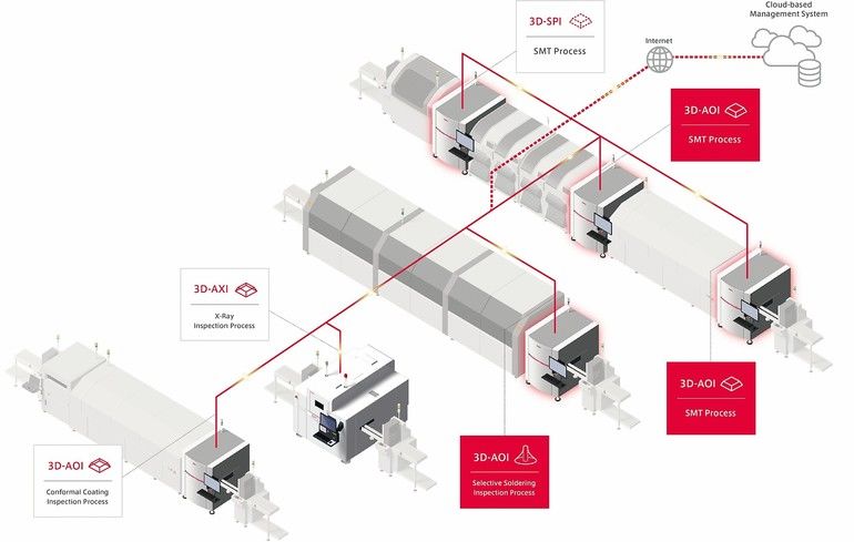
As the market continues to accelerate automation in PCBA back-end production, realizing the Smart Factory or Industry 4.0 is essential. Towards that end, Saki created a common software platform for SPI and AOI. Now their bottom-side AOI can also connect to other systems in back-end production. In the future, PCBA back-end production will have a similar configuration to an SMT production line, connecting other systems to feedback or feedforward information of defect points, to have better control of production quality. Together with the company’s advanced SPC and reporting feature, not only in the SMT production line, but also PCBA, back-end production will bring a comprehensive perspective to improving product quality in the production line.
productronica, Booth A2-259
Zusammenfassung
Da der Markt die Automatisierung in der Baugruppen-Backendproduktion weiter beschleunigt, ist die Realisierung der Smart Factory oder Industry 4.0 unerlässlich, wozu eine gemeinsame Softwareplattform für SPI und AOI geschaffen wurde.
Résumé
Le marché ne cesse d‘accélérer l‘automatisation de la back-end production des composants et rend essentielle de mettre en œuvre les modèles Smart Factory ou Industry 4.0. Une plate-forme logicielle commune pour SPI et AOI a été créée à cet effet.
Резюме
Рынок продолжает стремительно развиваться в направлении автоматизации производства бэкенда узлов, поэтому концепции умного производства или индустрии 4.0 все чаще реализуются на практике. Именно для этого и была разработана общая программная платформа для систем контроля нанесения паяльной пасты (SPI) и оптического контроля качества (AOI).


