The momentum for converting to Pb-free assembly processes is increasing with the approach of the WEEE and ROHS directives which will require electronic manufacturers in Europe to banish Pb beginning in 2006 or 2007, respectively. From the process point of view, what is necessary for a company to go lead-free? What are the areas of most concern?
Steve Dowds, Indium Corporation of Europe
Let’s begin our discussion with a survey of the variety of Pb-free alloys currently in use. Apparently, there is no direct drop-in replacement for SnPb solder; if there were something available which was as good as Sn/Pb, costing the same or less, and non-toxic, industry would already be using it. Every replacement alloy has some deficiency in terms of cost or performance when compared to Sn/Pb. For the sake of simplicity and pragmatism, since there are literally hundreds of Pb-free alloys that are either being used or put forward for consideration, we shall consider only the most popular alternatives.
Regarding the most interesting soldering alloys
Tin-bismuth (58Bi42Sn, 138°C) – The low melting point makes this alloy attractive, since there is a lot less thermal shock to the assembly during reflow and less energy is required, which is helpful for environmental considerations, too. However, this is an extremely brittle alloy with very poor shear strength. This can be improved by doping the alloy with 1%Ag, but the shear strength is still only 70% that of SnPb. Moreover, this alloy is sensitive to Pb-contamination.
Tin-silver-bismuth (various compositions, 200 to 210°C) – This alloy type has seen a lot of use in Japan, particularly on consumer-electronics products which are not subject to adverse operating environments. The concern with these alloys is Pb-contamination; adding just 1% Pb to an SnBi joint will cause the joint fracture strength reduction by 80%. These alloys show excellent wettability, superior even to SnAgCu, and have theadvantage of requiring a lower peak processtemperature. Once lead is completely out ofthe system, SnAgBi may prove to be the best choice.
Tin-zinc (91Sn9Zn, 199°C) – This alloy was first developed in the 1920’s as a solution to the problem of how to solder to aluminum, and, for that application, it is very good. It is attractive as a replacement for SnPb because the constituent metals are inexpensive and it has a low melting point. Unfortunately, zinc reacts likewise with acids and bases, and as a result, solder paste containing this alloy has a very short shelf life. Even storing the paste at -40°C (like conductive adhesive) does little to extend shelf life. NEC in Japan has used SnZnBi in a notebook computer, but it is difficult to imagine this alloy becoming a mass replacement due to the short shelf life.
Tin-copper (99.3Sn0.7Cu, 229°C) – A promising alloy for wave soldering, as it is cheap. However, it is not so suitable for use in SMT reflow lines, as the melting point is too high. One problem with this alloy is copper absorption. An SnCu-solder bath will absorb copper from OSP boards that pass through the wave. The phase diagram for SnCu reveals that a 2% increase in Cu content will increase the melting point of the solder from 229°C to approximately 250°C. If not carefully controlled, this could be a catastrophe. The alloy will corrode steel when it is liquid, so damage to wave-guides and pumps are likely. However, austenitic steels (for example, 316L, stainless steel) are not corroded by molten tin below 400°C. The use of those steels for machine parts will prevent corrosion.
Tin-silver-copper (95.5Sn3.8Ag0.7Cu, 217°C) – This alloy is widely recognized as the most suitable choice in the short to medium term for Pb-free soldering. The addition of Cu to Sn/Ag reduces the melting point, improves wettability and appears to give increased long-term reliability. Another point in its favor is that it is not as sensitive to Pb-contamination as Bi-containing alloys, and can be used with SnPb-plated components with no major problems.
There are a number of competing patent claims and a number of competing compositions. One composition, 95.5Sn4Ag0.5Cu, is „open“; i.e. it is prior art from 1950, so no one can patent it. The best advice is to ensure that a paste supplier has legal access to all the appropriate licenses.
Next step: looking after the other main process topics
Having chosen the alloy, we have to then consider many other topics of high influence on the process. Components are a concern, since many are simply not rated for the higher process temperatures that Pb-free alloys require. Large components will need at least withstanding temperatures of 230 to 235C in order to properly provide a reflow procedure. On a board with a very large thermal mass, the delta T across the assembly may be as much as 25K or more. Therefore, we can expect passive components to see as much as 250 to 260C. With careful process control and the right choice of flux chemistry, larger components such as QFPs need not see temperatures higher than 235°C.
Another consideration is that as the peak temperature increases, so too does the effect of moisture inside the component. If a component is rated as having a moisture sensitivity level of 3 (MSL3) at a peak temperature of 225°C, if the peak temperature is increased to 235°C, that will increase it to MSL4. Many components which are not sensitive in the current SnPb-process, will be so when the move to Pb-free is undertaken. Baking of components prior to use will become more frequent, in order to avoid problems such as popcorning or cracking.
Then we have to look at solderability. SnPb has a low surface tension (about 300dyne/cm), so it spreads easily. Often the assembly we are putting together has an SnPb-finish on the PCB, with an SnPb-coating on the component leads. Once the oxides are removed, the atomic structures are similar, so everything coalesces quickly. Wetting is also helped by the fact that we use 35 to 40K of superheat. When using SnAgCu we have an alloy with a higher surface tension, approximately 500 dyne/cm, so it does not spread so easily. The dissimilar metals of SAC paste, NiAu or OSP board finish, possibly leads to immersion Sn component finishes, and also less superheat is needed, typically only 20K.
Instead of simply removing the oxides and having a simple coalescence assisted by lots of superheat, we now have dissimilar metals with minimal superheat and a higher surface tension. The result: less spreading and a joint that is not as shiny as we expect with SnPb. It is important to remember that it is not a worse or less reliable joint.Simply stated it only has a different appearance, so education of operators and inspectors will be necessary.
Process issues
The minimized superheat we have to work with means that reflow profiling becomes critical. It is familiar for an engineer attempting to use one profile for a ‘family’ of assemblies of similar size, even though layout and component mix may vary significantly. This is usually workable with SnPb, as we have a generous pro-cess window. As long as all the assembly reaches about 200°C, we can be reasonably confident that everything will flow and solder. With Pb-free alloys, due to the temperature restrictions imposed by the upper limit of components, we have a much smaller reflow-process window to work with. Depending upon the flux chemistry, a window of as little as 10K may be all we have to work with. So careful profiling of each assembly becomes critical.
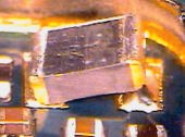
The widespread rules of good design and the same logical approach to troubleshooting still apply, but one thing to be aware of is that there are two very common problems when moving to Pb-free soldering: tombstoning (figure 1) and voiding (figure 2). We know that tombstoning is caused by differential wetting across the ends of the two-pole components, and it used to be a very frequent defect in vapor-phase soldering. Reduced tombstoning compared to SnPb was expected with Pb-free, as SnAgCu has a much lower wetting speed than SnPb. But practical experience has shown that tombstoning is more likely. This can be attributed to the higher surface tension of the alloy; it has a greater „pulling“ force on the component terminals, despite the slower wetting speed. With careful profiling and adherence to good design rules, tombstoning can be avoided.
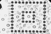
Increased voiding (particularly with BGA and flip-chip components) is well-known, particularly when SnAgCu-paste is used with SnPb-plated component ends. This occurs because we need to reach 230 to 235°C peak temperature to reflow the solder paste, but the SnPb-plating on the components will endure 50K of superheat for 2 minutes or more. Oxidization occurs much more rapidly when the alloy is liquid, and the resulting higher oxide levels cause more voiding. In general, SnPb-plated component terminals with SnPb solder show less voiding than SnPb-treated components with Pb-free paste. Conversely, Pb-free components with Pb-free alloy will also show less voiding. Careful control of the profile preheat stage can minimize the size of such voids, if not their number.
Best way to lead-free manufacturing process
The best route to Pb-free soldering for most users is probably the following, when using an appropriate SnAgCu alloy:
- 1) Select and introduce a Pb-free board finish
- 2) Perform solder-paste evaluation and selection
- 3) Perform pilot builds using Pb-free boards and solder paste, but employ existing components
- 4) When Pb-free components become available, introduce them
- 5) Most importantly, start with smaller, less complex assemblies to gain confidence
- 6) Define your rework process. While the assembly is „mixed“ (Pb-free paste and board, SnPb-plated components) SnPb wire can be used; when the assembly is entirely Pb-free, the rework process should also become Pb-free.
The lessons learned in step 5 will allow easier implementation on larger and more complex assemblies. If your production consists of large complex assemblies, start looking at Pb-free now; the day for implementation is not too far away.
ZUSAMMENFASSUNG
Nach der Auswahl der Bleifrei-Paste ist der Anwender noch nicht auf der sicheren Seite im Prozeß. Denn noch muß geklärt werden, welche Oberflächen-Endbehandlungen weisen Leiterplatte und die unterschiedlichen Bauteile an ihren Anschlüssen auf? Hier kann es bei einem Mix zwischen bleifrei und bleihaltig zu äußerst unerwünschten Effekten kommen, die zu Baugruppen-Defekten führen.
RÉSUMÉ
Il ne suffit pas à l’utilisateur de choisir une pâte sans plomb pour être du bon côté du processus. Car il lui faut encore déterminer les traitements de surface que présentent la carte imprimée et les différents composants au niveau de leurs contacts. Le mélange avec et sans plomb peut avoir ici des effets extrêmement indésirables, conduisant à des défauts des sous-groupes.
SOMMARIO
Dopo la scelta della pasta senza piombo l’utente non è ancora passato sulla parte sicura del processo. Infatti, rimane ancora da chiarire quali trattamenti finali sulla superficie mostrano i circuiti stampati ed i vari componenti costruttivi nei loro punti di collegamento? Qui non sono da escludere degli effetti particolarmente sfavorevoli in seguito alla miscelazione di paste senza piombo e con piombo, che possono causare molto spesso dei notevoli difetti dei gruppi costruttivi.
Share:


