There was a time when the actual layout of a printed circuit board (PCB) did not have much impact on the way it worked. As long as the components fitted on the board and the assembler could make it, functionality was not affected. With surface mount technology (SMT) and continuing technology breakthroughs, operating frequencies are even getting higher. As they increase, the impact of individual features on a PCB, such as the track layout, assume much greater importance as they affect the functionality of the design.
Dave Burrell, Senior Technology Consultant, Plextek Ltd
As frequencies and their resolution increase, problems can start. When frequencies jump to exceed the 1.0GHz level, it may also become necessary to change to a different substrate material that has a tighter toleranced dielectric constant to improve performance. These sorts of materials are typically PTFE (soft substrate) or ceramic-loaded PTFE.
Some of the functional problems that begin to manifest themselves as frequencies increase include:
• The proximity and lengths of individual and adjacent tracks can have an inductive or capacitive effect, causing signal coupling
• Extra spur tracks to provide test access produce similar effects
• Finishes, including the resist on the PCB, can influence transmission line properties
• Via holes which provide local grounding can look like inductive components to the circuit
• In-circuit test pins can act like small antennae
Therefore, it is vital to minimize these problems in order to meet the twin objectives of desired functionality and good product yield. RF designers and manufacturing engineers must work hand in hand to keep costs to a minimum. By having these two teams working together concurrently during the design phase, it is possible to strike a compromise between the different needs of the two disciplines – ironing out all potential problems before they get anywhere near the shop floor. Typically on RF designs, the designer will sit with the PCB layout engineer to highlight the critical areas, but the manufacturing engineer must do the same. This three-way discussion is extremely important, and can minimize the risk of having to re-spin a board layout. An RF circuit typically is not tolerant to intrusive testing, and once working, one cannot afford to make significant changes to improve test access and yield problems.
Basic principles affecting layout and performance
In order to work in the best way with the design team, the manufacturing engineer must understand some of the basic design principles. By doing this, he can recognize the designer’s requirements and why these are so important to the functionality of the design.
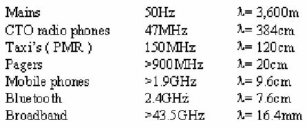
Frequency increases will affect the way the board is laid out and the overall design. For example, 50Hz mains, a sinus-oidal wave, is oscillating at 50 times per second (just fast enough to not see a light bulb flashing). However, a GSM mobile phone, which works at 900 or 1800MHz; will oscillate at 900 million cycles per second or even twice. It is important to understand the wavelength of the signal (the physical distance between one sine wave peak/or trough and the next). The actual effective wavelength of the signal is relative to the speed of light in air. However, the signal is here not passing through air but across a substrate. The actual material, whether FR4, PTFE or ceramic-loaded PTFE, will have its own effect on this owing to its ‚dielectric constant‘ and loss factor value or, in other words, how much it absorbs some of the signal. Consequently, as the frequencies get higher, the design may need to use more exotic materials which will alter the effective wavelength (l) but provide less signal loss, as well as providing more consistent performance.
As an illustration: wavelength at 50Hz on FR4 is about 3,600m. Clearly, feature changes are not likely to have much impact at this frequency. However, by looking at the table, it can be seen that as frequency increases, the wavelength gets smaller and smaller until the potential for PCB features to have an impact starts to become significant.
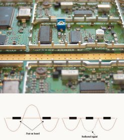
But how does this actually influence what happens on a PCB? Figure 1 shows a screen wall assembly, which is mounted to a DECT phone product, with small standoff feet forming the solder attach medium to the PCB. The distance between these feet has been calculated so that the operating frequency of the product (1.8GHz) will not pass through the gaps.
When waves travel across the surface of a PCB as demonstrated in figure 1 (bottom), a half-wave gap will allow signals to easily pass through. However, if the gap is decreased to l/4 or less, then signals will tend to be internally reflected and will not escape the frame. External interference at this frequency will also be reduced. Furthermore, not only the primary wavelength needs to be considered, but also its higher harmonics, requiring a gap suitable for 1.8GHz to be only 5mm.
Techniques and finishes affect PCB function
It is not only the tracks and the physical items on the PCB that can cause problems for the RF functionality of the circuit. As previously discussed, the wave is traveling along the track/surface of the board, and there is a field that is being generated around the track as it travels. Part of this field is being ‚propagated‘ within the PCB substrate itself (the reason why different materials affect it), and the rest is being propagated in the air above it. The signal will travel at a given velocity with a defined amount of loss/inefficiency, which is dependent on the length and the shape of the track and the medium through which it is traveling – in this case air, copper and FR4.
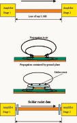
Manufacturing design rules require a solder resist over the top for pad definition, to stop solder bleed, and this can cause a problem. This results in a signal that no longer only propagates in air, but also in the resist. This would typically increase losses because air has low loss and the resist has even more. Also, the resist thickness is too variable for its effects to be calculated accurately. Hence, impedance could be variable, and this could cause incalculable circuit performance changes. So a compromise is needed. Rather than coating the whole of the track in resist, an answer could be to put a short bridge of resist adjacent to the component only (figure 2). Not only will this minimize the amount of variable effect, but also it will still enable solder processing control provided by the solder dam.
This technique works well in association with gold over nickel finish. It is often used on our designs, where there is no other choice due to the high-frequency nature of the product. Alternatively, selectively plated nickel could be used overthe track to form the barrier, but this is expensive on volume product, and nickel can be a difficult material to use around RF.
PCB track sizes are important
In typical RF PCB designs, some of the tracks need to be much wider than others. Additionally, in some cases, if the RF designer has laid out the PCB with no concern for thermal effects, that may lead to ‚tombstoning‘. It is possible that there will be components (typically passives) which have a track of, say, 7-mil (175 micron) entering at one end, and 20-mil (500 micron) exiting from the other. Components with different size tracks entering and exiting is a prime example of how ‚tombstoning‘ or ‚billboarding‘ can occur, and is something that the manufacturing engineer must watch out for. Different track widths affect impedance, and matching the size of the track to the correct impedance (say 3mm for 50 lines on FR4 ), is important for circuit performance. This type of track is commonly called a microstrip line, and will typically have a ground plane directly underneath it.
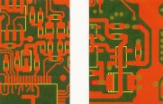
The impedance of the track depends on its width, the thickness of the track, the distance between the underside of the track and the ground plane, and the dielectric constant of the substrate material itself. Furthermore, the length and width of tracks also makes them appear like small inductors or capacitors respectively, asfrequencies get higher. The PCB layout shown in figure 3 reveals a typical copper imbalance problem which can appear if not kept in check during the design phase.
Clearly, there is reasonable risk of ‚tombstoning‘ here, especially as components work their way down to 0402 and 0201-sizes. However, there is a simplesolution. If the design needs the topend of these components to have the 20-mil wide track, then there may be potential to make the track at the other end thesame size (locally at least). This gives both the designer and manufacturer what they want, and actually improves the design.
As discussed, features on the track can also have capacitive or inductive effects. Because of this, it is often the case that the design will require grounding connections to be as short and as efficient as possible. The result of this will typically mean that one end of a component has a normal pad going off, for example, to a 5-mil (125 micron) track, but the other end will be sitting on an enormous ground plane with a thermal mass 100-times greater. Of course, this is a major disaster on the shop floor – the thermal mismatch is enormous and the component will tip up during reflow. Therefore, it is important to minimize this by discussion with the designer as early as possible. As shown, the high-mass end of the component could be thermally isolated. However, it is important to note that this must be discussed carefully with the designer, as the small links can still have ‚parasitic‘ effects which are small but significant inductive effects.
Test access problems can be avoided
Most companies that provide board test solutions will agree that methods of verification are changing. With the progress of constant product miniaturization and high frequencies, the opportunity for getting into a board intrusively to test it is becoming increasingly difficult if not impossible. The tester companies offer an abundance of solutions such as in-circuit, functional, flying probe, boundary scan or vector testing.
The lack of space now being provided for ICT pin access to be adjacent to component terminations poses a problem. With lower frequencies, bringing a spur track off could give access but, with higher frequencies, this will add capacitive parasitics, possibly making the functionality of the circuit different from the original design. Furthermore, even if the track itself had no effect, putting an ICT probe onto it may load the circuit, so altering its performance, and working like a small antenna. Typically, high frequency circuits use low value capacitors and inductors and, as a rule, ICT equipment cannot measure down to these levels anyway.
Realistically, test coverage by traditional methods is starting to reduce. Getting at the test nodes is difficult, and even if there are some nodes that the engineer must reach, then he may need to sacrifice access to some of the others to achieve it. The example in figure 4 shows this kind of predicament, where the proposed stub created to provide test access would have been in parallel to an existing track feature, which could not be moved. If this had been allowed then there may have been ‚coupling‘ between the two features, thus altering the circuit performance.
The way to remove the mystique of RF design
It is of ever-increasing importance that the manufacturing and testing groups talk very carefully with the designer in the initial stages of a product to determine the test strategy. Without being able to get test access by traditional ICT methods, what are the alternatives to check the assembly functionality? Perhaps for some of the boards boundary scan is possible, but this will not help much with the peripheral passives and some of the other discrete components. Maybe automated optical inspection will meet some requirements or flying probe tests – but then pad sizes will have to be suitable for flying probe (very small outlines are used on mobile products). However, it may be possible to use functional cluster test methods.
In summary, the old analogy of RF circuit design being a ‚black art‘ does still apply to an extent. However, manufacturing engineers must take care to prevent this ‚mystique‘ allowing the RF design to compromise the manufacturability of a product. By talking at the product concept stage to determine the test strategy, and by working with both the RF designer and the PCB layout designer during product development, such compromises can be minimized.
Zusammenfassung
Übliche Mikroprozessoren takten mittlerweile mit maximal 2,5 GHz (der Bustakt im PC liegt aber „nur“ bei maximal 400 MHz) und Mobiltelefone funken mit 1,8 GHz. Unter solchen hochfrequenten Umständen kommt dem Design der Leiterplatte und damit der darauf montierten Baugruppe höchste Bedeutung zu, damit kritische Hochfrequenzprodukte sowohl effizient mit hoher Ausbeute fertigbar sind als auch ihre Funktionalität gewährleistet ist. Bereits in der Konzeptphase einer Baugruppe müssen sich Entwickler, Fertigungs- und Testspezialisten über viele Fragen einigen, bis hin zur abschließenden Verifikation von Fertigungsprozeß und Produkt.
Résumé
Les microprocesseurs usuels atteignent aujourd’hui une fréquence maximale de 2,5 GHz (alors que le bus dans le PC n’autorise „que“ 400 MHz maximum) et les téléphones mobiles 1,8 GHz. A de telles fréquences, le dessin de la carte imprimée et du circuit qu’elle supporte revêt une importance capitale pour la rentabilité de fabrication des produits haute-fréquence critiques et leur fonctionnalité. Dès la phase de conception, les spécialistes du développement, de la fabrication et du test doivent se mettre d’accord sur de nombreux points, y compris sur la vérification finale du processus de fabrication et du produit.
Sommario
I tradizionali microprocessori nel frattempo hanno velocità di clock di massimo 2,5 GHz (mentre il clock del BUS in un personal computer corrisponde „soltanto“ a massimo 400 MHz), mentre i telefoni cellulari trasmettono ad una frequenza di 1,8 GHz. In simili condizioni ad alta frequenza il design del circuito stampato e con ciò dei componenti su di esso montati acquisisce una massima importanza, affinché i prodotti ad alta frequenza siano producibili sia in modo efficiente, con un elevato fattore di sfruttamento, che con la garanzia di un massimo di funzionalità. Sin dalla fase progettuale di un componente di costruzione, gli specialisti addetti allo sviluppo, alla produzione ed ai test devono chiarire molti fattori, partendo dal processo di produzione, al prodotto finale fino alla verifica conclusiva.
Share:


