Silicone materials have a unique combination of properties which make them well suited to chip-scale packages (CSP). Their use can bring significant advancements in device reliability and longevity. Silicones now have an established track record in production of flash memory devices, SRAMs and DRAMs. Dow Corning is using a number of methods to reduce the cost of ownership (COO) associated with packaging, and provides a pricing roadmap, contributing to their position as the preferred supplier.
The world of device packaging is constantly in motion, and the search for the next „best package“ design never ceases. The most recent industry shift is from thin, small-outline packages (TSOPs) to an increased use of CSPs. A very familiar type of chip-scale package is the BGA, using a flexible tape and compliant silicone elastomer design to create a package with the optimum combination of reliability and performance. The compliant assets of the BGA materials allows decoupling of the CTE mismatch within the package, maximizing the life of solder balls. The small size of these CSPs also reduces the signal path from the silicon to the system, improving performance and offering significant savings in board real estate. Design wins and selections as benchmark package have driven the growth of BGA to the point where25 million parts per month are currently being manufactured using this technology.
Current cost reduction efforts
As the technology has matured and assemblers have reached higher volumes, the BGA has become essentially a drop-in replacement option, with a goal of delivering the optimum combination of performance, reliability and package cost. With increased use of this technology, Dow has been able to take advantage of higher volume manufacturing techniques, larger equipment and more automated processing to reduce labor costs and turnaround time, with subsequent cost benefits to CSP manufacturers.
In addition, improvements in raw material costs have been negotiated with suppliers through the benefits of volume purchasing, and the long shelf life of the current generation of materials (a year from the date of manufacture) helps eliminate scrapping of outdated products. The overall cost reductions should make the design more attractive to contractors who have until now been excluded from the advanced packaging playing field due to development cost, high risk and lack of infrastructure, all of which are eliminated through the use of BGA technology.
CSP cost in TSOPs versus flip chip
In general, the industry has developed two measuring sticks: TSOP for high volume packaging, and flip chip for advanced/ high performance packaging. The BGA design can fill both these needs, making it imperative that the costs associated with manufacturing the BGA are well understood, and that a cost roadmap is developed to move this package into more cost-competitive territory.
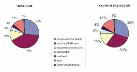
The pie-type charts in figure 1 show that material cost makes up about 60% of the total CSP cost in the SRAM design, and nearly 70% in the DRAM package. With this understanding, it is apparent that suppliers of the encapsulant can make the biggest impact on cost, die-attach adhesive and substrate.
The previous cost roadmaps for BGA designs are not seen as progressive enough to entice new users, or in some cases, to warrant continued use in existing CSPs. The question to ask is: at what price per-formance? The BGA is a proven pack-age with an impressive track record, and the sacrifice in reliability from using aless robust package can be very detrimental. Still, DRAM is a commodity business with extremly tight margins and manufacturers are requiring a more progressiveroadmap.
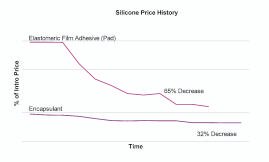
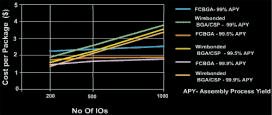
Using the latest pricing roadmaps from Dow, a 32% decrease for the encapsulant and a 65% decrease for the film adhesive are shown over time (see figure 2). Taking this projection and using it to calculate the package cost, BGA comes in at ~$0.6 for a 144M RDRAM at a volume of 3 million packages per month. Higher volume can bring this cost down to ~$0.45, still viewed a high premium when compared to current TSOP packaging that can be made for ~$0.3, and this is the comparison that most DRAM manufacturers are making. The difficulty in this exercise is the fact that TSOP designs will not meet the high performance needed for advanced packaging. The second comparison is to flip-chip designs, which have always been a very expensive option, and are typically not specified for high-volume DRAM packages (see figure 3). The cost of flip chip is ~50% greater than of traditional chip-scale packaging at DRAM I/Os.
Is solder bumping on substrate attractive?
At least two major reasons have been identified to explain why directly attaching the solder-bumped flip chip on organic substrates has not yet become popular. First, because of the thermal expansion mismatch between the silicon chip and the epoxy substrate, an underfill encapsulant is usually needed for sufficient solder joint reliability. However, the manufacturing cost is increased and throughput is reduced, due to the underfill procedure. In addition, the exchange of an underfilled flip chip on PCB during rework is very difficult, if not impossible.
The other issue cited is that the pitch and size of the pads on the peripheral-arrayed chips are very small, posing great demands on the supporting substrate. High-density boards with sequential build-up (SBU) circuits connected through microvias are not commonly available at reasonable cost. Indeed, supplying reliable underfill between die and package, and doing it quickly, has slowed the migration of flip chip to the midrange IC realm. Every cent is important in the backend of the chip business, and slow underfill steps have proven too costly.
The BGA system has an extensive network of proven equipment, and materials readily available from an extensive list of suppliers. This enables a new adoptee to get up and running very quickly. Additional efforts and acknowledgement of competing CSP technologies will continue to drive cost down, eliminating the need for multiple packages.
One of the obvious requirements is that assemblers work closely with materials suppliers to understand how the material cost comes into their process. Significant improvements can be made in the BGA, including one already in use: densification of the TAB tape. According to Craig Mitchell, VP of memory products business at Tessera, the company’s licensees have realized a two-fold cost savings through densification of their strip design. In addition to process changes, new materials are also being developed, which can eliminate the need for multiple die attach steps.
Reduction of waste
The next step is reduction of waste generated during the tape conversion process and maximizing production efficiency. Dow Corning is working with tape converters to find novel ways to affix the die-attach film, which may remove cost from the system. In a similar vein, the encapsulants and wet die attach media are currently shipped in syringes, but equipment modifications that enable the use of larger packaging will have a positive effect on total cost of ownership.
Of course, there are many other CSP types to choose from, and some customers are using multiple CSPs for the same device. However, there appears to be little argument that the BGA has outstanding board level reliability, viewed by many as the best performing, most reliable CSP on the market. With a competitive cost structure, the design can eliminate the need and cost associated with having device duplication.
In addition to process changes, materials are constantly being developed. These products can eliminate the need for multiple die-attach steps, offer faster cure and lower viscosity, all of which can increase throughput, thus lowering the overall package cost. With Dow’s global technical support, users have access to analytical and testing capabilities to resolve characterization issues or other questions. Materials are available for a variety of technologies and configurations: elastomeric film adhesive (pad), liquid die attach and encapsulants in a wide range of viscosities, all qualified in BGA production.
Zusammenfassung
Mikroelektronik-Silicone sind besonders gut geeignet für Cip-Scale-Packages, denn sie bringen deutliche Verbesserungen in puncto Zuverlässigkeit, Kosten und Langlebigkeit. Speziell fürs Verpacken von Speicherbausteinen liegen ermutigende Aussagen vor, wobei es keine unterschiedlichen termischen Materialausdehnungen zwischen Chip und Substrat gibt. Damit entfällt das aufwendige Underfilling.
Résumé
Pour le moulage des boîtiers de semi-conducteurs, on a utilisé des polymères ou des matières à base de silicone, ces dernières se caractérisant par leur grande flexibilité après le durcissement. Les avantages des silicones sont nombreux. Outre la protection contre les influences de l’environnement, ces matières absorbent également par exemple le stress mécanique dû aux différences de coefficient de dilatation thermique des matériaux du chip et du stratifié.
Sommario
Per la fusione di packages di semiconduttori é possibile utilizzare polimeri o materiale su base siliconica, materiali questi ultimi caratterizzati da un’alta flessibilità dopo l’indurimento. I siliconi offrono molti vantaggi. Oltre alla protezione dagli agenti atmosferici il materiale funge anche come tampone contro lo stress meccanico, generato a causa dei differenti coefficienti di dilatazione termica tipici dei chip e dei laminati.
www. dowcorning.com/electronics
Share:


