Increasing expectations and demands from customers of electronics equipment mean that the manufacturing technologies behind these devices are also propelled forwards. Powerful wearables, the Internet of Things (IoT), mobile communication devices, and new huge data storage subsystems are pushing the semiconductor industry and electronics designers to new heights, and production specialists are now encountering the limits of their inspection machines. As we can see, electronic devices are getting smaller and smaller, and, ideally, losing a bit of weight, whereas performance is being continually enhanced.
Ever more semiconductor manufacturers are adopting advanced packaging technologies, and heterogeneous integration is a hot topic, especially when it comes to designing systems in a package. Advanced packaging is among the fastest evolving areas of the semiconductor industry, featuring even smaller component sizes, lower power consumption, and remarkably increased I/O connectivity for providing more functionality. The various advanced packaging options, such as System-in-Package (SiP), Fan-out wafer-level packaging (FOWLP), 2.5D, 3D chip build-up, and so on, have, of course, added the necessary flexibility and performance to many applications. As customers demand more sophisticated functionality in smaller devices, the application of delicate components is a necessity. It is important to keep in mind, however, that all these advancements come at the cost of increased package complexity such as adding more layers, even finer features, and more I/O channels.
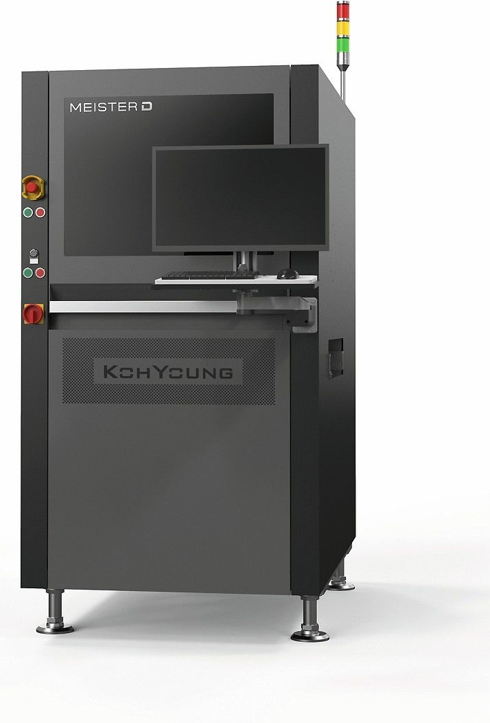
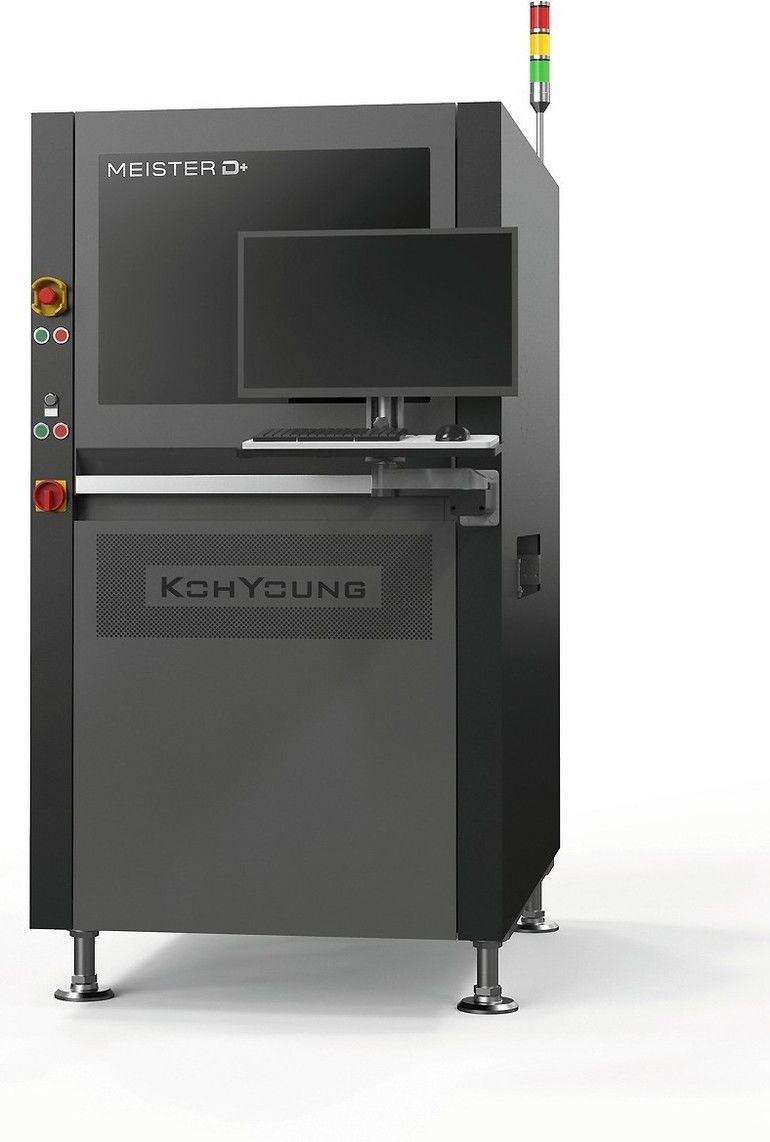
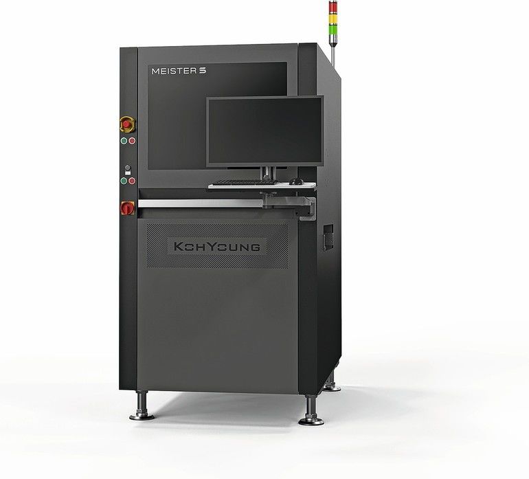
With ever larger and tougher requests from the technical side, inspection and quality control processes in both the semiconductor and the electronics manufacturing industry are going to become even more critical. New packaging technologies and solutions are far more demanding than those semiconductors used before. Inefficient or inadequate manual or semi-automated and time-consuming methods of inspection and quality assurance must be replaced with powerful systems which are meeting and even surpassing the requirements of today‘s electronics components. It should not be forgotten that aging standard SMT inspection systems (AOI) may now be reaching their limits when it comes to providing sufficient resolution for very small printed solder pads with the required accuracy and repeatability. It is clear that a brand-new generation of inspection technologies which can provide optimum solutions for the continually increasing complexity of the industry is necessary. With this in mind, Koh Young, the leading provider of 3D measurement-based inspection solutions, has now launched the systems Meister S, D, and D+; these systems deliver unsurpassed levels of repeatability and accuracy for the verification tasks of advanced packaging devices at semiconductor fabs as well as in the electronics manufacturing industry.
Next level integration of functions
Semiconductor packaging technology has been evolving constantly and rapidly to support increased device density, functionality, and I/O connectivity. Yet Moore’s Law (which states that the number of transistors will double in dense semiconductors every two years) has been slowing down for the past couple of years. The number of transistor functions of a component such as a microprocessor, once used as a benchmark, is no longer increasing at its former pace. The rate of acceleration is slowing down after more than 30 years of continual progress.
Previous development in chip technology was focused on miniaturization and complexity. The trend now is to include more versatile, sophisticated functions in a wide variety of different applications. At the same time, cost-effectiveness, performance, and higher integration are becoming of higher interest as the market demand for novel devices which provide ever more functionality to customers increases.
It is unsurprising, then, that ever more manufactures are adopting SiP component configurations, which feature the splitting of functions into single blocks, and result in a couple of tiny single components mounted in one and the same compact package. This technique can enable higher integration and consequently lead to size reductions for embedded systems. In contrast, the approach of System on a Chip (SoC) diverges significantly from this integration method as all functions implemented in SoC components are integrated onto the same single die.
Defect challenges growing in
advanced packages
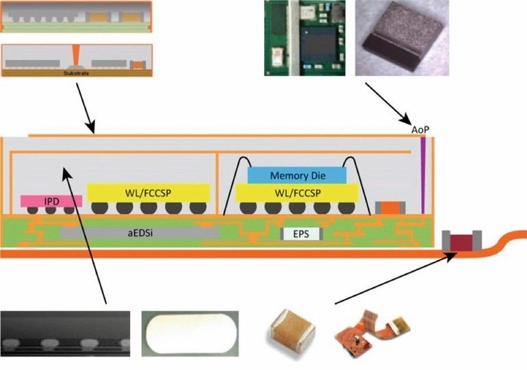
As processes and features become highly delicate and complex with more layers and I/Os, the source of possible defects in the package is getting smaller, making them harder to inspect using the current systems on the market. With the miniaturization of electronic devices, the processable areas of a wafer must be used optimally in order to get the high yield required. The number of components on a single wafer disc increases exponentially with every shrinking step of their geometries. Higher component density brings about a particularly demanding situation, because not only do the components become smaller but their higher density on a wafer disc also leads to disturbing shadowing effects which render an efficient and precise inspection almost impossible with traditional instruments.
For years, the industry had relied upon 2D solder paste inspection (SPI) and automated optical inspection (AOI) systems to locate visible defects. However, this conventional 2D inspection is significantly challenged by certain aspects of today‘s semiconductor applications. Shiny die surfaces can diffuse inter-reflections, which may create an unacceptable level of uncertainty between the height and tilt of the surface. The inability to detect defects with high accuracy has a direct impact on yield figures. And it should not be overlooked that the cost of an undetected possible production failure can increase dramatically, especially when health and safety concerns are involved – such as in the case of automotive advanced driver-assistance systems (AADAS) or other sensitive applications.
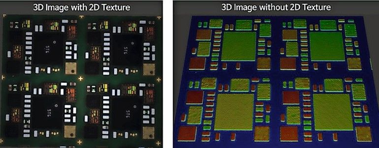
Indeed, electronics manufacturers are encountering huge difficulties with the inspection of shiny components using 2D and 3D techniques. To solve this issue, Koh Young has developed the novel Meister D/D+. With these systems, users can overcome these critical challenges in the manufacturing line by employing a full and uncompromised 3D inspection and 2D inspection for secure verification of demanding failures of all kinds, including very fine cracks and even foreign material inspection.
The systems Meister S, D, and D+ combine the proven Moiré technology and modern optical configurations to reliably support the inspection of shiny components in 2D and 3D. With their newly developed technology, they are the perfect fit for the inspection of SiPs on SMT electronic board assemblies, among other critical applications. The brand-new systems feature this extra capability as an expansion of Koh Young’s superior AOI technology with a different optical system configuration compared to the Zenith series (different lighting system).
The latest Meister system is optimized for the inspection of dies and ensures the fastest, most accurate measurement with an 8-projector inspection probe tailored to typical SiP components including microchips and tiny chips. The shadowing problems caused by small and narrow gaps are a thing of the past. The very high precision of the inspection results is assured by the camera subsystem featuring 25 MP and 3,5 um resolution. With ongoing miniaturization, the requirements for higher resolution inspection systems are also increasing. At least 100 pixels must be available for a single repeatable measurement of the finest and smallest feature. Also, the flatter angle of the projection units enables the measurement of low heights and compensation of interfering reflections.
The system allows full and uncompromised 3D inspection of dies, as well as of cracks on 0201M (008004-in) SMDs. The new evolution is based on Koh Young‘s proven inspection technology, now employed in a novel way and available for other critical tasks. In basing the new solution on the proven platform, Koh Young made sure that its customers can expect extremely reliable results with the highest possible confidence. Accurate measurements are guaranteed. And, as such, the user benefits of the Meister systems are clear. With their high accuracy, these systems drastically minimize the number of unidentified defects and, in turn, increase the production yield with a secured higher quality. As it comes down to the in-sight of all electronics manufacturers, having more accurate data on the localization of possible defects in the early stages of production is key for adding value and saving costs.
Conclusion
Advanced packaging is becoming much more prevalent in the market, thanks, in part, to its advantages over traditional device packaging methods. However, board complexity and shiny die surface make the inspection process in the manufacturing line more challenging. The industry requires a high-precision inspection solution to overcome these challenges. When looking for the appropriate system to choose, it is of very high priority that the product manufactured is known in detail, then the decisive criteria can be set, and the optimum equipment solution can be selected.
With a competent partner as the solution provider, finding a capable and appropriate system meeting the requirements of advanced packaging is not rocket science. It is of the utmost importance that customers are able to rely upon a solid and trustful partner who provides suitable experience of the market, technology, and process demands. Koh Young, the leading 3D measurement-based inspection solutions provider, has now launched the Meister S, D, and D+, the next generation of systems for extended repeatability and accuracy for use with even more sophisticated advanced packaging devices.
 Source: Koh Young
AT A GLANCE
In this article, Koh Young explains how its Meister Series systems can help overcome the challenges associated with advanced packaging inspection.
Zusammenfassung Résumé Резюме


