Single-pass reflow encapsulants (SPRE) with various glass transition temperatures Tg below the 125°C were the subject of an investigation. The material with the lowest Tg (65°C) exhibited the best reliability, passing over 1000 cycles of liquid-to-liquid thermal shocks (LLTS -55 to +125°C). The result indicates that the encapsulant Tg and the coefficients of thermal expansion (CTE) are important, but not critical to the reliability of flip-chips assembled with single-pass reflow encapsulants.
Serge Tuerlings, Kester Solder Europe
For smaller and lighter electronic products, flip-chip technology with its higher I/O count and reduced package footprint will be required. As with any upcoming technology, other materials are needed. This is the driving force for significant developments with encapsulation materials. In order to attain high-volume production requirements, flip-chip encapsulants will need to be processed concurrently with traditional surface mount technology (SMT) devices (SMDs). The use of single-pass reflow encapsulant (SPRE) for flip-chip assembly operations provides significant advantages over traditional capillary-filling processes. The application of SPRE material allows assemblers to simplify the process from two steps to one. This is accomplished by combining the soldering and underfilling procedures into one step. Process time, equipment and overall cost can then be minimized.
Another key development in flip-chip assembly operation is the elimination of flux and underfill compatibility issue. By having the flux and encapsulant combined in a single material, there are no negative interactions left, directly or indirectly affecting the reliability of the assembly. To combine the flux and underfill tasks into one process step, the fundamental chemistry design requirements for such a SPRE material must be re-examined. An innovative single-pass reflow encapsulant, with both fluxing and underfilling capabilities, has been formulated to utilize compression-flow processing in SMT assembly operation.
As with any encapsulating process, including also this one, the glass transition temperature (Tg) and the coefficients of thermal expansion (CTE) are material properties of importance. It is widely believed that the deformation from expansion and contraction of the encapsulants directly relate to the reliability of the flip-chip package. To minimize the amount of deformation of the encapsulant during reliability tests, the Tg is often required to be greater than the high-end of the temperature range, typically 125°C. The CTE is often required to be as low as possible to minimize the mismatch of the properties of flip-chip package materials. Upon first glance, the lower Tg and higher CTE values of reflow encapsulants are immediate issues of concern, but through innovative chemistry of SPREs, the CTE and Tg can be properly balanced to fulfill stringent reliability requirements.
Four different SPRE formulations with similar chemical compositions but different Tgs (65 to 105°C) were investigated. This range is lower than what is generally considered to be acceptable for traditional capillary flow flip-chip encapsulants. However, the encapsulant with the lowest Tg value (65°C) showed some of the best reliability and passed over 1000 cycles in liquid-to-liquid thermal shock (LLTS) testing. This result questions the necessity of pre-determined Tg and CTE points being based on the theory where the high Tg is above the thermal cycling temperature range and the low CTE matches the die and board CTEs. With reflow encapsulants, Tg and CTE values can then be considered as important but not critical to the reliability of flip-chip package.
The experiment and its test conditions
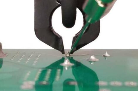
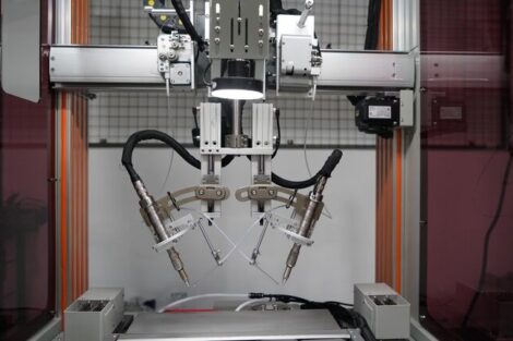
A 250×250-mil daisy-chain die and FB250 board from Flip Chip Technologies were used for our research. The dies had 48 I/Os, 63Sn37Pb solder bumps with 18-mil (0.45mm) pitch. The bump diameter was 7.5-mil and the bump height was 5.5-mil. The die had a polyimide passivation layer. The test substrate itself was 62-mil thick FR-4 board with 7.6×7.6-mil Cu/Ni/Au pads. Each board contained ten die sites. With an Asymtek Century dispenser featuring a positive displacement pump head we dispensed the SPREs to the substrates, using an X or cross-hair dispersion pattern. The dispensed volume was pre-calculated based on a machine-supplier program. The dispensing operation was done at room temperature. A Universal GSM-1 pick&place machine was used for placing the dies onto the test substrates.
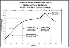
A Heller 1700 oven with a typical SMT reflow profile (figure 1) was used for reflowing the solder bump to form the electrical connection between die and substrate. At the same time the single-pass reflow encapsulant cures, forming a mechanical bond between die and substrate. A Sonoscan D-6000 C-mode scanning acoustic microscope (C-SAM) was used to investigate for voids or air entrapment within the encapsulant gap between die and the substrate after reflow.
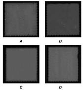
A Finefocus high resolution X-ray inspection system was used to verify the quality of the solder joints, to control that proper wetting and alignment have been made. X-ray inspection can also aid in determining if too much wetting has taken place in the case of non-soldermask defined pads. And a Blue-M thermal cycle chamber was used for the LLTS reliability test. The temperature range has stretched from -55 to 125°C. The hold time for each temperature extreme was 5 minutes and the transition time was less than 10 seconds.
Assemblies were tested in real-time for electrical opens and for adverse changes in the resistance values. A failure due to resistance increase was recorded when 10 events have occurred within the previous 10% of the cycles. An event is defined as a resistance change of 1000 for 200 nano-seconds.
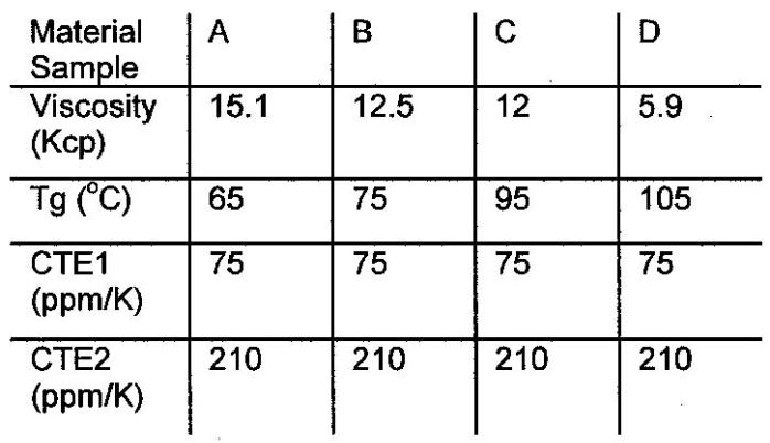
General property information on the four SPRE materials that were used in this research is shown in the table. Kester Solder supplied all these four single-pass reflow encapsulants.
X-ray inspection study
Upon close inspection with the X-ray equipment, all the solder joint areas showed signs of good wetting. The images reveal that the flip-chip bump had collapsed after reflow, giving the oblong shapes (as seen in figure 2). Proper wetting can be seen as darker circles or shadowing. This was due to the alloy being thicker in those areas. There was no bridging between any of the solder joints. After reflow, we performed electrical tests to check the solder connections between the dies and substrates. The resistance readings were very low for all the test vehicles. Therefore, it is believed that the solder joints with all four different encapsulant material sets soldered well under the standard reflow profile.
LLTS covering wide temperature span
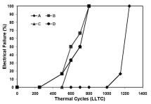
Each test vehicle was sent to the LLTS chamber for reliability testing. All these substrates were taken out of the chamber for evaluation after 500 cycles and approximately every additional 100 cycles. The reliability graph (see figure 3) shows that a small percentage (15%) of the C and D sample sets started failing prior to 500 cycles but reached 100% failure at 800 cycles. While the B material sample achieved better results earlier in the cycling, it eventually followed the same trend as samples C and D. The substrates with the B material completely failed at 800 cycles. Sample A showed first failure at 1100 thermal cycles, which was much better than all of the other sample sets. The A material showed rapid failure to N100 at 1200 cycles.
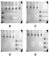
Image verification with C-SAM study
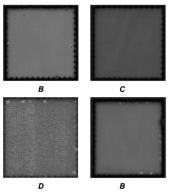
From the initial C-SAM images (scanning acoustic microscope), the test materials were dispensed evenly in the test vehicles material sets (figure 4). There were no major voids discovered in the encapsulant area on any of the material sets. Only one test die site was found having two small satellite voids around the solder joints. These were found in material A. This was the only die site in set A where voiding was witnessed. This particular die site was followed in the following photos after additional thermal testing.
After 500 LLTC thermal cycles, the C-SAM images show the C and D samples had some limited white spots around the edges (figure 5). The presence of the white spots indicates that delamination at die and substrate interfaces had started before 500 thermal cycles. This corresponds to the electrical reliability results showing that the C and D material sets started to fail at that time.
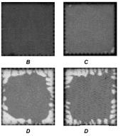
Sample material A shows no delamination in the C-SAM images after 500 thermal cycles (figure 5). The two satellite voids around the solder joints did not expand, nor did any additional delamination develop during the thermal cycling. There were no electrical failures for material set A. There was also no delamination shown in the scanning acoustic microscope images of the sample B after 500 cycles, and the electrical reliability results didn’t show any failure at that time. All of the test vehicles were also analyzed under C-SAM after 1000 thermal cycles. Material set C and D show significant delamination (white areas) around the edges (figure 6). The photos indicate that the delamination was developing from the corner fillet edge towards the center. The electrical reliability showed that all the test vehicles had failed for material sets B, C and D.
Material B exhibited limited delamination (small white spots in the corner areas) at the 1000 thermal cycle mark. However, all the test vehicles failed electrical verification. Material A die still did not exhibit any delamination under C-SAM (figure 6). The two satellite voids around the solder joints maintained the same size as prior to thermal cycling. There were no electrical failures in material A until 1100 cycles. C-SAM imaging analysis along with the real-time electrical tests showed that the delamination under the die relates with the electrical failure of the test vehicles. The delamination starts at the edg e of the die and develops from here to the center.
An outlook
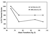
It is widely believed that high glass transition temperature (Tg) and low coefficients of thermal expansion (CTE are required for the encapsulation of flip-chip devices due to the difference in thermal expansion rates. This belief would allow only for testing of materials with Tg above the high-end of the thermal cycling range. For telecom use, flip-chip encapsulant would require Tgs above 125°C. However, as clearly seen in figure 7, the lower Tg single-pass reflow encapsulant exhibited better reliability than the relatively higher Tg materials within the same chemical family. The results confirm that a single-pass reflow encapsulant (SPRE) does not require high Tg in flip-chip application to meet high reliability standards. The lowest Tg (65°C) material (sample A) exhibited excellent thermal reliability. The data indicates that a high Tg is not a valid requirement to the reliability evaluation of single pass-reflow encapsulants on flip-chip assemblies.
References
D. Blass: Flux Issues For Flip Chip Assemblies, Universal Instruments Area Array Consortium, October, 1999
J. H. Lau and C. Chang: How to Select Underfill Materials For Solder Bumped Flip Chip on Low Cost Substrate, International Journal of Microcircuits & Electronic Packaging, Vol.22, No.1, 1999
R.G. Werner, D.R. Frear, J.DeRosa, and E. Sorongon: Flip Chip Packaging, Proceedings of the 1999 International Symposium on Advanced Packaging Materials, Braselton, GA, Mar, 1999
Flip Chip Calculator, www.asymtek.com
EIA/JES D22-A106-A Thermal Shock
Tomaso and H. Wang: Reflow Encapsulant for Flip Chip Application, Proceedings of APEX 2000
Zusammenfassung
Bei der Montage von Flip-Chip-Bausteinen, bei der ein Silizium-Chip umgedreht und mit einem Kunstharz-Laminat verbunden sowie mit Pads verlötet wird, mußten bisher dafür separate Prozeschrittte für Reflowlöten sowie Dispensing und Curing von Underfiller vorgesehen werden. Mit nun formulierten Single-Pass Reflow Encapsulants lassen sich Arbeitschritte und Kosten reduzieren. Eine Untersuchung geht auf die Einflüsse von Laminat-Glaspunkt-Temperatur und die Materialausdehnungskoeffizienten ein.
Résumé
Dans le montage des composants flip-chip, au cours duquel il faut retourner une puce de silicium, la lier à un stratifié de résine synthétique et la braser, il était nécessaire jusqu’à présent de prévoir des étapes séparées comme le brasage à reflux de même que le dispensing et le curing d’underfiller. Les single-pass reflow encapsulants actuels permettent de réduire les phases de travail et les coûts. Une étude s’intéresse aux effets de la température du stratifié et sur les coefficients de dilatation des matières.
Sommario
Nel montaggio di componenti modulari Flip-Chip, dove avviene un collegamento all’inverso di un chip di silicio con un laminato di resina sintetica nonché la saldatura con Pads, finora erano necessari passi processuali separati per la saldatura a riflusso nonché il Dispersing e Curing di sottofiltri. Con i Single-Pass Reflow Encapsulants ora formulati è possibile ridurre i passi di lavoro e con ciò i costi. Un’analisi si interessa sugli influssi della temperatura nel punto di transizione dello strato vetroso del laminato e sui coefficienti di dilatazione del materiale.
Share:


