With cost-effective substrates that are now available, flip-chip technology is conquering the volume market and making its mark as a future standard of connecting technology. The production equipment required here must provide high precision coupled with high processing speed. Choosing a machine partner is based on process and solution expertise, as well as modular production concepts and a strategically oriented platform. Here we focus on high-volume, low-cost flip-chips, manufactured in reel-to-reel operation.
Achim Pajonk, Datacon, Austria
Trends in electronics are currently converging from three directions: increasing price pressure on cost-critical, established high-volume manufacturing processes; a growing demand for new kinds of mass-market products (smart label, for example); and finally the increasing maturity of flip-chip technology. On the other hand, as flip-chip assembly becomes cheaper thanks to cost-effective flex substrates and the use of improved adhesive technology, many innovative product ideas are now becoming attractive in economic terms, so that manufacturers of embedded electronic products can profitably open up new fields of application with high user benefit.
Flip-chip devices for high volume products
Many electronics manufacturers are considering employing the flip-chip assembly process for their products, so that they can capitalize on all the advantages of this technology, including: maximum packaging density; good high-frequency properties; fewer connectors because of direct-chip assembly (DCA), low overall height, and high productivity of the assembly operation.
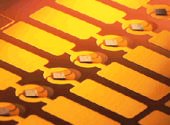
The target markets for such products are distinguished by high-growth momentum, with two major surges expected soon. One is flip-chip on board, similar to the familiar placement of SMDs on circuit boards: The other surge can come from smart cards or labels in various, usually ultra-thin style, which can range from so-called intelligent paper to high-frequency ID systems (figure 1), to pin-on medical electronics systems for health care.
These products emerge on the one hand from established flip-chip users who already have some experience with the technology, but also from innovative newcomers who have not become involved in this type of assembly so far, and also do not yet have the proper equipment for it. For these companies, the entrance barrier for the advanced technology is somewhat higher, but can be more easily overcome with experienced partners. Here, equipment suppliers such as Datacon with its extensive expertise from many customer projects and interdisciplinary research and development activities, play a key role. With their technological and organizational process knowledge, modular machine concept and a future-oriented equipment platform, they can get together with the customer to work out the optimum processes for an application, guarantee quality and ensure rapid startup of volume production.
Different flip-chip attaching methods
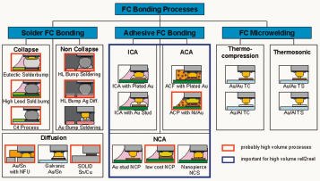
Which bonding/attaching technology of flipped chips is suitable for the mass market? This question is not easy to answer, as it depends on many factors. But a look at the diversity of the available technologies (figure 2) reveals important criteria that should make the decision easier. In principle, we really need to ask ourselves two questions: which of these processes could be suitable for mass production, and which of these processes allow reel-to-reel production?
Two of the three types of bond/attach process – soldering, adhesion and micro welding – are possible candidates for flip-chip assembly in high volume (figure 2, marked in red). For mass production, the individual process steps must be composed to form a production line providing a continual throughput, working, for example, from the reel. This limits the choice of the process to those which can be used in conjunction with low-cost substrates. For reasons of temperature, the procedures involving soldering must be eliminated here. This reduces the choice of bonding procedures (blue marked).
In this blue-marked field are two red-marked processes which are suitable for both volume and reel-to-reel production: conductive adhesive bonding and electrical connections with direct contact and isolating adhesive. Originally, bonding of flip-chips with anisotropic conductive adhesive (ACA) was developed for attaching on substrates that cannot withstand the melting temperature of eutectic lead-tin solders. The adhesives used are made up of polymers, e.g. in paste form, which contain conductive particles, for example small gold-plated polymer balls. If the contact surfaces of chip and substrate are pressed closer together than this diameter with the ACA-material be-tween them, then the now trapped balls create an electrical connection. Under pressure and exposure to heat, the adhesive is then cured and forms a fixed mechanical connection, eliminating the need for underfill.
Assembly with non-conductive adhesive (NCA) is based on the direct contact of chip pads and contact surfaces on the substrate, whereby the adhesive is also cured under pressure and temperature. It is clear that a number of critical parameters come into play here, which must be optimized for high process and product reliability during the joint process design by user and device manufacturer. Thus, process development and device technology ideally go hand in hand.
Modular, productive flip-chip production line
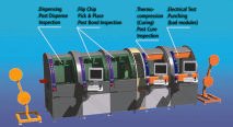
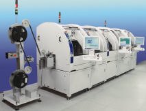
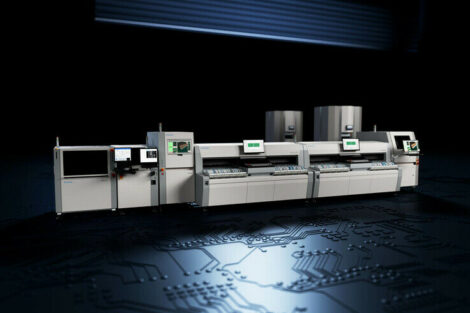
While mature equipment is available for existing flip-chip processes, the now emerging flip-chip assembly techniques for high-volume production require equipment which is tailored to the process and are, above all, flexible (figure 3). Particularly for new users of flip-chip technology, turnkey solutions from the experts promise high-quality processes and products but also fast startup of volume production. Such a high-throughput, high-precision production line, as for example the proven process modules of Datacon’s 2200 apm series (figure 4) includes various units: dispenser module with post-dispense inspection, flip-chip die bonders with integrated post inspection, thermo-compression module for the curing of the ACA-material with subsequent optical inspection, and finally the concluding electrical test, after which failing components are punched out. The reel-to-reel transport system extends over all modules.
The transport system works with block indexing, which complies with the slowest process step – in this case the thermo compression. To ensure careful handling of the substrates, as few index stages as possible are used in order to prevent the chips from slipping on the substrate. Defective devices, identified by punch marks, are located and excluded from further processing such as epoxy application and chip bonding. Because the supplied tape rarely comes in one piece, splices are unavoidable. To prevent the bond positions on these splices from being assembled, the transport system features a splice-recognition function.
The dispenser module at the beginning of the line works block-indexed with the die-bonder rate, and features special performance characteristics such as stable process flow, high-volume constancy, a positioning accuracy of ±50µm, processing of adhesive products in a wide viscosity range, and automatic height calibration for the dispenser needle. In the die bonder, the flip chips are picked up and positioned on the substrate with high precision and flexibility.
Because the curing process takes most of the time, it basically determines the process time. To increase the throughput, it is therefore performed on several components simultaneously. Several thermodes are operating in parallel, whose temperature is regulated exactly to within *1KC. To protect the thermodes from contamination by any adhesive projecting from the edge of a chip, a protective film is placed between thermode and chip. While the substrate is being transported, this film is automatically counted forward by one block. The pressure is implemented via the servo drive of the Z-axis and the spring-loaded thermodes. The various protective functions here include switching off the substrate heating if pro-duction is interrupted.
Each process step is accompanied by a concluding check. This in-line inspection ensures a high yield also in the introduction phase of a new technology, because any problems which occur are detected immediately. Datacon offers a particularly efficient inspection option for transparent adhesive.
The inspection function in the dispenser module recognizes failed or displaced adhesive applications based on the geometry of the applied epoxy pattern. The post die-bonding inspection focuses on the positioning precision, either with spot checks or 100%; the latter is recommended especially for the start phase of production. Following the thermo compression, the progression of the epoxy is inspected for failure or drift. The final electrical test of all parts assures the information about manufacturing quality. With the approach of flip-chip production systems on a flexible, modular and thus extendable equipment platform, Datacon aims to strengthen the competitive position of its customers by low cost of ownership.
Developing optimum processes and setting up novel production lines for innovative flip-chip technologies, introducing them quickly and successfully, and operating them economically for large production runs require not only a product supplier but also an expert solution provider who knows the customers‘ processes and offers wide-ranging process and production knowledge. Datacon has completed its internal expertise network of interdisciplinary projects with international partners. This competence has been quickly converted into economic successes for customers through the joint designing of processes, taking over complete process developments right through to supplying complete flip-chip lines for mass production.
ZUSAMMENFASSUNG
Die Technik ist bestechend: Ungehäuste Dies mit ihren Kontaktpunkten exakt auf die korresondierenden Pads auf dem Substrat aufsetzen und in einem Rutsch sind sämtliche Kontakte hergestellt. Doch für den hochvolumigen Markt, rein unter Kostengesichtpunkten gesehen, sind die vielen Montageschritte, die für die Herstellung des Flip-Chips-Gehäuses nötig sind, nicht ideal. Einfachere Verarbeitung von Rolle zu Rolle mit eingesparten Prozessschritten kann interessante, heute noch nicht bekannte Anwendungsbereiche erschließen.
RESUMÉ
La technique est séduisante: poser des Dies sans boîtier avec leurs points de contact exactement sur les coussinets correspondants sur le substrat. En un clin d’œil, tous les contacts sont réalisés. Toutefois, pour les gros volumes, ne serait-ce que du point de vue des coûts, les nombreuses étapes de montage nécessaires pour la fabrication du boîtier de la puce flip ne sont pas idéales. Un traitement plus simple selon l’application avec des étapes de processus économisées peut ouvrir la porte à des domaines d’application encore inconnus aujourd’hui.
SOMMARIO
La tecnica è seducente: basta applicare i Dies privi di alloggiamento esattamente sui rispettivi Pads del substrato ed ecco che in un batter d’occhio sono stabiliti tutti i vari contatti. Ma per il mercato di volume elevato, dal puro punto di vista dei costi, i vari passi di montaggio necessari alla produzione di alloggiamenti Flip-Chips, non sono affatto ideali. Una lavorazione semplificata da rotolo a rotolo risparmiando passi processuali può rappresentare interessanti campi d’applicazione finora ignoti.
Share:


