
Optimised processes and increased productivity are the aims achieved by a producer of solar cells by using the Inspector 2D vision sensor. The easily parameterised device inspects extremely thin silicon wafers, and the subsequent photosensitive solar cells, for broken edges with great precision – ensuring that they are detected and rejected as early as possible in the production process.
Thomas Hall, Technical Manager, Electronics Industry, Factory Automation Solution Centre, Sick AG, Waldkirch, Germany
Whether solar technology; the semiconductor industry; or microsystem, medical and circuit board technology – higher levels of efficiency, optimised process chains, maximum process reliability and guaranteed product quality are achieved wherever defective parts are diverted out of a production process in good time thanks to a dependable vision sensor. The solar and photovoltaic industry, in particular, currently faces heavy demand – necessitating efficient and comprehensively automated production and inspection processes for solar cells. Since most of the sector has undertaken the first automation step – connecting processing stations and machines with one another – the next step is to optimise processes and increase production.
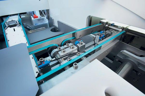
A world market leader in wet chemical inline and batch processes for the production of solar cells wanted to exploit these potential improvements, e.g. by means of the early detection of damaged wafers and solar cells passing through the machines. The production of solar cells made from silicon wafers takes place in a series of complex steps. Differing layers are placed upon the silicon substrate in a variety of wet chemical, plasma and thermal processes. As the resultant cells are very thin (with a thickness of about 200 µm), the risk of damage during transport and handling in the plant, as well as from process-related mechanical and thermal stress, is correspondingly high. For this reason, the company was looking for a solution to inspect wafer and cell edges for damage during insertion into machines and while leaving them.
The Inspector investigates in difficult circumstances
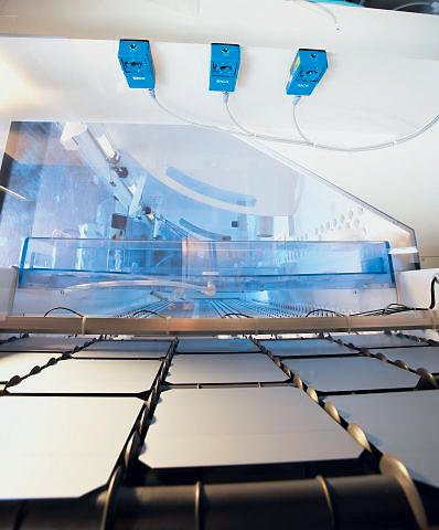
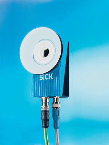
Whereby two requirements were particularly important: firstly, easy mechanical and electrical integration of the inspection sensor in the plant; secondly, detection performance adapted to the inspection task, taking into account that the surface and appearance of the wafers or cells changes after almost every process step – from a shiny silver to a deep blue, almost black, colour and with either mono- or polycrystalline structures. The early detection and subsequent ejection of damaged units from the production process was solved with the Inspector – a compact, user-friendly and reliable 2D vision sensor with integrated illumination, image evaluation and Ethernet interface. This all-in-one design makes the highly integration-friendly Inspector the application-oriented parameterisable solution for numerous tasks. The ring of LEDs integrated in the metal housing – with its enclosure rating of IP67 – illuminates all areas of the cells (i.e. also the process-critical edge regions) homogeneously and with almost no shadows.
Position-independent inspection on several lanes
Rough alignment in the field of view is sufficient for inspecting the edges of the 156 x 156 mm² wafers and cells that pass the measurement field of the Inspectors in several lanes and at a distance of about 500 mm. Regardless of position and orientation, the sensors’ software algorithms evaluate all edge areas – within a few milliseconds and with the necessary accuracy. No trigger signal is required – detailed inspection of the object takes place as soon as it has been detected in its entirety. During the inspection of wafer breakages, the achievement of a minimum pixel sum in the measurement windows focused on the four edge areas determines whether a particular wafer is good or not. A particular part is diverted out of the line if one of its edges is damaged. This ensures that only “in order” cells pass through each processing step.
The Inspector offers many advantages. The sensor is easy to operate and, as an alternative to the ring LEDs, offers the possibility of integrated dome illumination – of particular benefit for glossy, highly reflective surfaces. An Ethernet interface and time-optimised image evaluation also support use of the Inspector in more rapid processes. Settings that have been programmed can be stored on a PC and copied into other Inspectors with the same task. For this purpose, the Inspector offers a variety of possible configurations – from signal-controlled teach-in to external teach-in of a new part contour and PC-supported configuration, which allows rapid teach-in in a few steps. Edge inspection is therefore just one of many potential uses in the solar cell sector. Thus the Inspector can be used to inspect labels or logos on the cells, or for inspecting breakages on defective cells in a variety of transport and handling tasks within the production chain. In each case, the Inspector is a highly economical solution: the sensor is not only considerably more reasonably priced than a complex camera solution, it can also be much quicker and more easily integrated and adapted to process or measurement changes in production.
More sensors for the solar sector
Automated production processes for solar cells are essential in order to be able to satisfy the high demand. Apart from the Inspector, other sensor solutions from Sick’s portfolio also make a major contribution to the reliability and availability of these processes. Examples include optoelectronic, electromagnetic and ultrasonic sensors in handling systems, as well as during the identification of solar cell boxes, solar modules and individual solar cells. Then there are camera sensors and systems for checking dimensions and surfaces as well as for inspection tasks; and electromechanical or optoelectronic safety systems, e.g. on partly automated processing stations or even fully automatic robot cells. In each application, reliable detection by sensors from Sick ensures maximum throughput performance during the production of solar cells.
EPPE 428
Share:


