Desoldering QFN components is not much of a big deal. However, due to strongly varying residual solder amounts on the PCB, there are no defined conditions for safe and repeatable component placement into residual solder. An approved and preferably contactless site dressing solution is necessary to set the preconditions for fresh solder deposition. Direct Component Printing (DCP) turns out to be a very effective and time-saving method to improve high value QFN rework.
Flat packages such as QFN (Quad Flat No-Leads), sometimes known as MLF (Micro Lead Frame), have beneficial electrical and thermal characteristics and are increasingly incorporated into densely populated, space-saving printed circuit boards. In general, defect QFN components can be reworked. However, unlike BGA or CSP, they do not provide their own solder depot. Therefore, prior to soldering, the component’s contact areas and/or the corresponding pads on the PCB need to be supplied with a defined amount of solder. This determines certain demands on rework stations.
Desoldering QFN components is not much of a big deal. With respect to rework, they even offer advantages against BGA and CSP, as there is no need to consider particular aspects of solder alloy mixing during the reflow process. However, due to strongly varying residual solder amounts on the board, there are no defined conditions for safe and repeatable component placement into residual solder. Consequently, it is recommended to employ an approved and preferably contactless site dressing solution to set the preconditions for fresh solder deposition.
As mentioned before, the surroundings of QFN are getting increasingly populated. Thus the established way of locally applying solder paste with stencil and squeegee is not always practicable. On the other hand, dispensing high numbers of contacts is a slow process and the accuracy does not meet the demands. Moreover, there is a need to use specific solder pastes since not all of them are suitable for dispensing.
How to apply fresh solder material
The solution for easy, safe and quick solder paste application is provided by the QFN component itself. In contrast to BGA or CSP chips, QFN components have a perfectly flat underside. This allows, after flipping, solder paste transfer directly to their contacts, if proper clamping can be provided.
There are different methods to apply fresh solder onto the contacts. Their common objective should be hitting the right position and achieving a high level of uniformity. Then, after successful printing, there is still another challenge to cope with: How to handle a solder paste printed component without destroying the fresh print layout?
A common solution to protect the print layout is a separate reflow process in a reflow oven after paste printing on the component. Alternatively, a greater number of components can be provided with solder paste simultaneously via a ceramic transfer plate. A dispenser is used to apply the mirrored QFN pad array onto the ceramic plate, then the QFN components are placed above and the solder is reflowed to the contact pads.
A major drawback of the above methods is that both paste application approaches will have fresh QFN components going through a questionable extra thermal cycle prior to the actual soldering process. Every reflow step means additional thermal stress and will have an impact on quality and reliability of the component and its electrical connections, so it will be difficult to guarantee for OEM quality of the reworked assembly. Apart from that, limited availability as well as time and cost aspects go along with the paste reflow detour – not talk about the necessity of doing all steps in a closed ESD environment. According to IPC 610/JEDEC 001, QFN components may be exposed to not more than three reflow cycles.
Additional equipment is needed
Finally, both paste application approaches need additional equipment which is no integral part of a typical rework machine. In consideration of all mentioned aspects, direct printing of fresh solder onto the QFN component right before soldering is the recommended solution.
When combined with other essential rework process steps, Direct Component Printing (DCP) ensures an all-in-one solution for QFN/MLF components with pitch of 300 microns or below. Integrating residual solder removal, safe component handling and component reflow with optimized thermal profiling for the freshly pasted component will provide a smoother path to high-yield rework.
As paste printing will be performed at room or store temperature, no thermal issues are to be expected. The prior residual solder removal process makes for defined and even surface conditions on the board. Even in case the printing results should once fail to meet the requirements, room temperature cleanup can be done easily without leaving migrating solder pearls on the interconnect device.
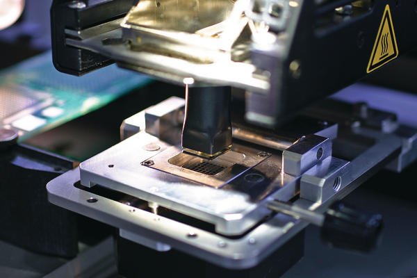
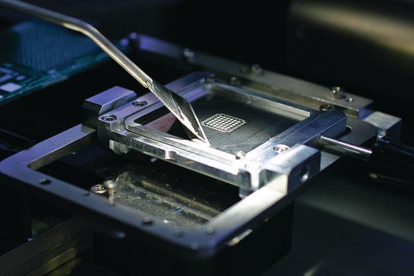
As the following description indicates, direct component printing is a sequentially stepped procedure using a Direct Component Printing (DCP) Module, integrated into the rework machine. Each step is designed to minimize the risk of paste smudging.
The component to be pasted is transferred to the die presentation via vacuum pipette and picked up from there by the soldering head. The openings of the stencil which is clamped in the DCP Module and the component’s pads are viewed through the Fineplacer split-vision optics and aligned. Now the QFN component is placed to the stencil and “snaps into place”. In the next step, the component is flipped 180°, so its contact pads will face upwards. Solder paste can now be spread with a squeegee in typical fashion. The thin-film stencil allows for an even paste application on the pads. Once the paste is printed, the printing result can be inspected via the Fineplacer’s magnification optics. Afterwards, the component is flipped back, so that its backside faces the reflow tool. At the end of the sequence, the component is picked up from the DCP Module. By using the precise Fineplacer optics, the pads are aligned to the substrate and the component is placed prior to reflow. No tool change is necessary, as the standard soldering head is used for the complete DCP sequence. This ensures that once the component is picked from the module, the process consisting of alignment, placement and reflow can continue automatically. Implementing nitrogen into the reflow process will improve the formation of an optimal solder meniscus.
Finetech’s DCP turns out to be a very effective, safe, easy-to-use and time-saving method to improve high value QFN rework yield with fine pitch beyond hand/eye dexterity limits. DCP becomes integral part of the rework cycle and can be performed within any Finetech rework system equipped with the DCP Module. Unlike other paste application approaches, no additional reflow step is necessary which contributes to avoiding thermal stress issues and saves both time and money. It is guaranteed that the reworked assembly can be provided in OEM quality. Components without own solder deposit will only go through one reflow process.
EPPE412
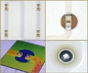
No visible contacts
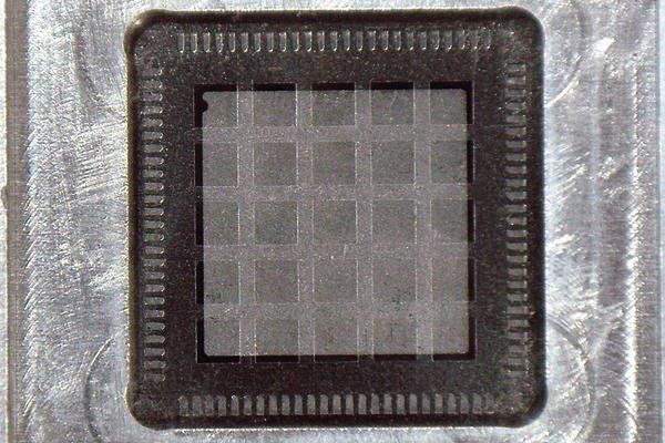
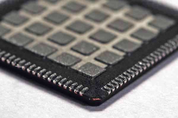
A QFN (Quad Flat No leads) is a SMT package similar to the Quad Flat Package, but the leads do not extend out from the sides of the package. The perimeter lands on the bottom of the package provide electrical contact to the PCB. The leadframe’s metal die-attach paddle on the bottom of the package allows for a stable, low-impedance ground, as well as heat transfer to the PCB. QFNs are mainly used in mobile and other high-dnsity applications.
µ-assemby and rework with advanced packages
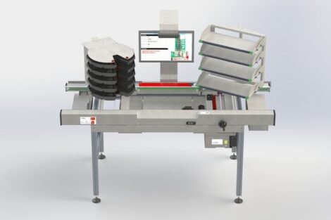
Finetech is a leading manufacturer of innovative rework and micro assembly equipment for the latest advanced packages. The modular design of the Fineplacer platform enables a multitude of applications, from reworking SMDs to the highly accurate placement of flip chips or opto-electronic components. Finetech is headquartered in Berlin/Germany, with offices in Tempe/AZ-USA, Shanghai/ China and Kuala Lumpur, Malaysia.
zusammenfassung
An Reparaturvorgänge mit QFN-Komponenten kann man selten mit Standardregeln herangehen. Das Auslöten ist zwar einfach, doch anschließend müssen Bedingungen geschaffen werden, dass das erneut einzusetzende Bauteil auch sicher und qualitativ hochwertig kontaktiert werden kann. Denn diee Bauteile besitzen kein eigenes Lotreservoir. Für diese Aufgabe hat sich das Direct Component Printing-Verfahren (DCP) als sehr geeignet erwiesen. Es ist zuverlässig und spart Zeit.
Il est rare de pouvoir aborder les travaux de réparation des composants QFN/MFL (Quad Flat No-leads/Micro Lead Frame) en appliquant tout simplement les standards. Le dessoudage est certes simple mais il faut ensuite créer les conditions nécessaires pour que le composant de remplacement puisse être connecté de manière sûre et dans le respect des critères de qualité. Le procédé Direct Component Printing (DCP) s’est révélé d’une aide précieuse dans ce domaine. Il est à la fois fiable et rapide.
Share:


