When it needs to be small and compact, the unique LDS process has something to offer: a laser treatment and subsequent metallization process create conductors on three-dimensional plastic bodies. LPKF is presenting new products at the Productronica that combine for fast and reliable prototyping for 3D molded interconnect devices. – LPKF Laser & Electronics Ag, Garbsen (Germany)
Complete system eases entry
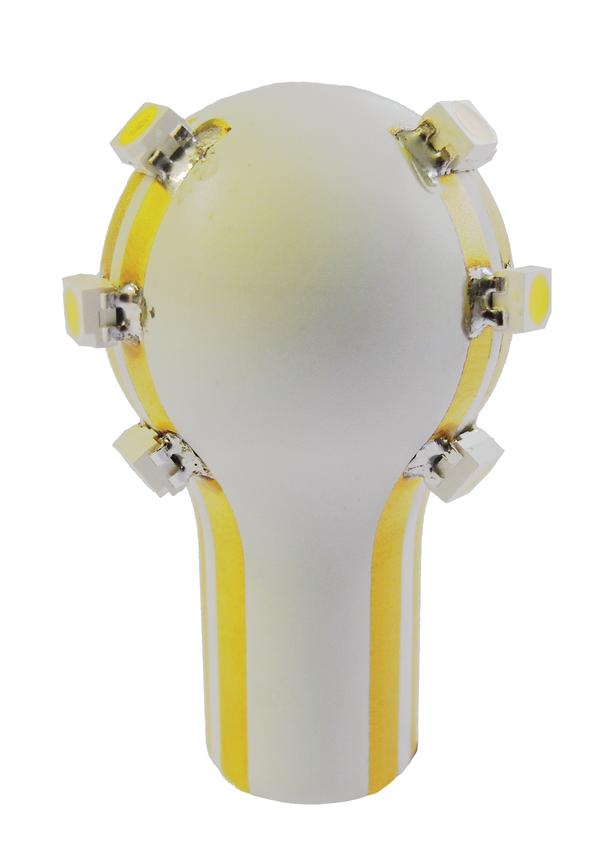
LPKF vice president Britta Schulz holds a black cube the size of a sugar cube and a tiny black disk the size of a lentil in her hand: both are pressure gauges for auto tires – before and after redesign as 3D components. The size of the component demonstrates the potential: its volume features merely a fifth of the predecessor because all connections are already structured into the component itself. Britta Schulz is sure that the market for three-dimensional molded interconnect devices will continue to grow strongly in the next few years. The LDS (laser direct structuring) process patented by LPKF has already achieved a market share of more than 50%. With the complete prototyping series, the German laser specialist is closing the gap between design and serial production.
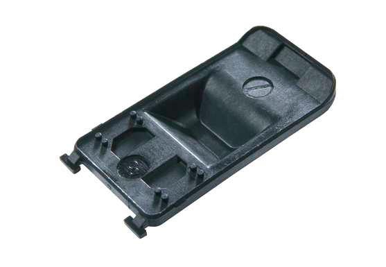
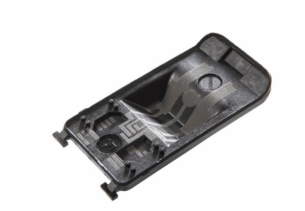
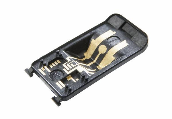
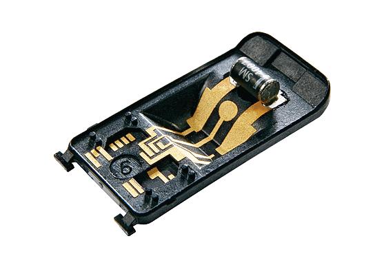
Three-dimensional molded interconnect devices are suitable for combining mechanical and electronic functions. The footprint and weight of the component are clearly reduced. Components take over mechanical and electrical tasks. Injection-molded plastic components serve as the foundation surface for mounting of the strip conductors. That is also why they are named molded interconnect devices (MID).
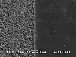
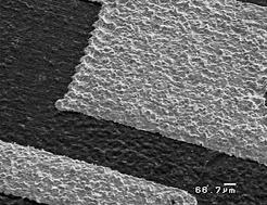
With the MIDs, LDS takes a leading position. Components that are produced from an additivized plastic are the foundation. All of the important plastic suppliers offer materials with an LDS additive now. The component is inscribed by laser. The laser treatment exposes the additive and creates a micro-rough surface for better adhesion of the strip conductors.
Then a current-less metallization bath builds up the strip conductors on the structured areas. With this process, strip conductor thicknesses of approximately 10µm are possible; a finish with nickel and gold can follow in the process sequence.
The LDS process
This state of LDS technology is well known and proven, and is established in automotive, electronic and medical devices. Every second smart-phone currently has at least one LDS component, with antennas being prime examples of the advantages of this technology. An emerging trend is the use in LED lighting – as spatially arranged LEDs are very close to the emission behavior of conventional light sources.
Producing LDS prototypes
Especially innovative and outstanding is now a complete new process for LDS prototyping. It closes the gap between design and serial production, where production quality prototyping has previously been too expensive and time-consuming. The basic idea of LDS prototyping is in creating an activatable surface by coating any component with a layer of paint. Plastic components from 3D printers, for example, can be used as base bodies. Important is that after painting a sufficiently smooth surface is created so as to achieve a continuous metallization. The printed base body is covered with a paint that contains LDS additives. With the new LPKF ProtoPaint LDS paint, a single thorough painting is sufficient. The paint is supplied in a spray can and is activated before the first painting.
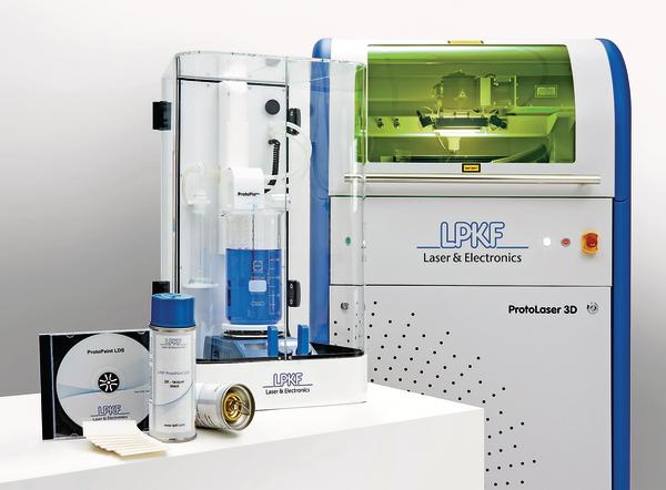
For laser structuring, LPKF launches a completely new laser system. It is based on the proven ProtoLasers and is equipped with a laser optic system which is also used with production systems. The ProtoLaser 3D requires only a wall socket and an exhaust. It has a height-adjustable work platform for structuring components of different dimensions. The working range is 300 x 300 x 50mm, and the scanning field is 100 x 100 x 25mm. Infeed of the component is ensured by a movable XY-table.
For metallization, LPKF is presenting another ready-to-use solution: the ProtoPlate LDS delivers current-less metallization of milled LDS components. It consists of a protective enclosure for process guidance and an already prepared combination of bath chemicals as consumables. The metallization process is as easy as making coffee. The base metallization is poured from the canister into a beaker and then heated to the working temperature of about 44ºC. An activator solution that is also portioned in advance starts the process. The components are then simply immersed in the bath. The thickness of the copper layer – usually in the range of 3µm to 10µm – primarily depends on the dwell time. After metallization, the consumed bath chemicals are put back into the canister, marked with a label that is supplied, and then can be easily disposed of.
Easy access to technology
Britta Schulz explains the way forward: “We are observing more and more interest in this technology and are expanding the area of use in a targeted fashion. We are lowering the entrance thresholds with the systems and processes for LDS prototyping. All systems are available after Productronica.” With the processes presented, samples for functional and installation tests can be created that are very similar to serial components. The LPKF subsidiary LaserMicronics is also organizing an LDS road show through German cities in the first quarter of 2014 in order to offer easy access to the technology.
LDS in industrial use
The ProtoPaint LDS is available as a paint system with separate components and as a spray can. The paint system has to be mixed and can be processed with the spray pistol or through printing. This variant is intended for industrial use, for example, for antenna structures on the back of monitors or smart-phone covers. The designers profit from the fact that they can use plastics with known surface or dielectric properties.
Chemical metallization is comparatively simple, but also has disadvantages. Galvanic reinforcement is available for mechanically stressed components or with thicker layers. First a thin metallization (3µm) is quickly applied. Then the component is electrically connected and galvanically reinforced. In practice, this process delivers layer thicknesses of up to 35µm with a smooth surface. Due to the more homogeneous layer, the hardiness to mechanical and thermal stresses is increased.
Still in the experimental stage, but with great potential: painting of metallic carriers with an LDS-capable coating powder. This process is especially suitable for LED applications because many design versatilities can be implemented due to the good thermal conductivity of the base body.
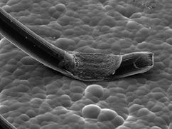
The resolution of 200µm (100µm line, 100µm distance) is already a peak value with three-dimensional molded interconnect devices. Electronics developers, however, often require even more. With an optional fine-pitch laser unit and with the ProtoLaser 3D, applications with 75µm/75µm (line/distance) are already in place; in the future even finer structures will be possible. These ultra-fine conductors are desirable, for example, in sensor systems or with stacks of ICs in molded interconnect devices.
Productronica, Booth B2.105
Zusammenfassung
Damit der patentierte LDS-Prozess noch leichter in die Fertigung überführt werden kann, stellt LPKF ein komplettes, neu konzipiertes System vor. Die Metallisierung von Kunststoffoberflächen benötigt eine Lösung zur Oberflächenvorbereitung, dann folgt die Laserstrukturierung und schließlich die flüssige Metallisierungsbasis. Diese Technologie für 3D-MID ist damit noch weiter auf dem Weg in die industrielle Nutzung.
Afin que le processus breveté LDS puisse être encore plus facilement transposé dans la fabrication, LPKF présente un système complet de conception nouvelle. La métallisation des surfaces en synthétique nécessite une solution pour la préparation des surfaces, intervient ensuite la structuration au laser et enfin la base liquide de métallisation. Cette technologie pour 3D-MID est ainsi encore plus avancée sur la voie d’une utilisation industrielle.
Share: