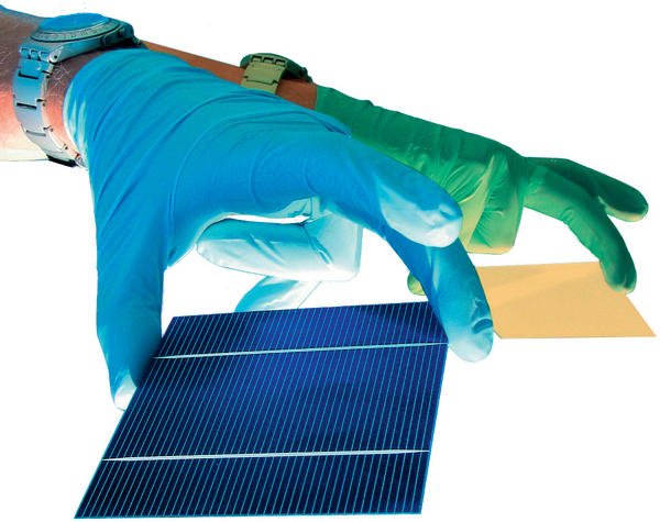
Capillary conducting paths, wafer-thin layers and micrometer precise drillings: The success of solar energy is determined by the tiniest of things, which result in overtime for the laser. Solar cells on roofs have progressed to become a status symbol. They protect the environment and they look chic – especially due to the silver shining conducting paths, which span the front side of the crystalline silicon solar cells like a net. But what pleases the eye does not necessarily please the manufacturer and their customers. This is because the conducting paths, which are positioned onto the semiconductor material using a screening process, and which discharge the load carriers, waste valuable surface space no longer available to collect sunlight – up to ten percent is lost due to these paths.
Higher yields Uwe Stute, Trumpf Laser, Schramberg, Germany
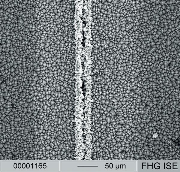

Engineers found a solution about 15 years ago. A laser etches grooves into the silicon, which are then filled with metal using a galvanic process. This costs only about five percent of the surface, making cell efficiency accordingly higher. “With the laser-grooved solar cells, laser processing in photovoltaics manufacturing was born,” remembers Andreas Grohe, head of laser and coating processes at the Fraunhofer-Institut für Solare Energiesysteme in Freiburg, Germany. Much has happened since then. Lasers are now used in the photovoltaics industry for drilling, cutting or removing layers – with an increasing tendency. This is mostly thanks to the market. The growth rate of the photovoltaics industry in the last five years was above 40 percent – per year. The laser industry should be cheering, and yet the exact opposite is the case. “Laser manufacturers often do not know what fantastic things they could make with their products when manufacturing solar cells,” Grohe observes surprised.
At the limits of mechanics
Sometimes companies are quickly discouraged – as, for example, with edge insulation. About four years ago, the entire solar industry converted to lasers in order to remove a few millimeter fractions of semiconductor material from the edges of the silicon wafer, which could otherwise lead to undesired short-circuiting around the edges, by firing it with light. Wet chemical procedures are now taking over the laser, and laser suppliers doubt whether the market is becoming overrated. This is not, however, the end of laser – much the opposite, according to Grohe: “The industry has to recognize that this was the first admission ticket into the solar industry and that many new applications are yet to be unlocked.” The Verband Deutscher Maschinen- und Anlagenbau VDMA also confirms this. Dr. Eric Maiser, Head of the “Forum Produktionsmittel für die Photovoltaik“ at VDMA, believes German suppliers are well equipped for the solar market: “Manufacturing processes in photovoltaics are similar to those in conductor board, semiconductor or display production – and German companies have a lot of experience in this area.” The times when crystalline solar cells, which still continue to dominate the market with well over a 90 percent share, are mechanically drilled or sawed, will most likely soon come to an end. Two trends are the door opener for the laser. One is that wafers are becoming increasingly thinner in order to save expensive silicon – the goal is 0.1 mm. The other is that manufacturers are aiming at a production rate of one cell per second, as well as production lines. According to the unanimous opinion of 130 specialists, who met last September in Hameln, Germany for the international conference “Laser Technology in Photovoltaics” this is almost impossible without the use of a laser. The fact that production costs for new production and cell concepts are increasing at the same time does not interfere, because the solar cell will quickly recoup these costs due to its higher energy yields. Ultimately, all development projects share a common goal: increase the efficiency of a solar cell, or, to be more precise, the performance yield per cost. Scientists at Germany’s Fraunhofer ISE in Freiburg developed a solar cell together with the Institut für Solarenergieforschung in Hameln, Germany, and a manufacturer, which accomplishes an efficiency of 21 percent instead of today‘s standard 17 percent. This was achieved by integrating four steps with laser processing into the manufacturing process.
The knack of the back side
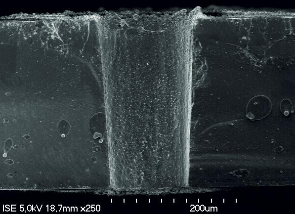
The Institut für Solarenergieforschung in Hameln, Germany, follows another concept. It installs the emitter contacts on the back side – this means there are no more conducting paths blocking the sun on the front side. Instead, tiny conducting holes in the silicon substrate allow the load carriers to flow from the front side to the back, where they are collected using standard metallic lines and are then fed into the electricity network. A lot of holes are required to keep the distances as short as possible, at least one per square millimeter. For cells with about 15 cm long edges, this represents up to 30,000 holes that can only be drilled with a pulsed infrared laser in a matter of seconds and at production speed. The surface loss caused by the holes is less than one percent. Another reason the silicon disks should be thin is that they can more effectively collect short-wave light that only penetrates the surface by a few millimeters. What is practical for ultraviolet light has disadvantages for long-wave infrared radiation, which penetrates a millimeter deep and partially leaves the semiconductor at the back, without contributing to electricity production. This is why aluminum is applied to solar cells from behind as a reflective coating. While aluminum has good reflection features, it also leads to recombination of the load carriers and therefore performance loss. A wafer-thin layer of silicon oxide between the actual energy producing layer and the aluminum would be ideal, as this would prevent the recombination. This layer must, however, be opened to allow contact with the conductive paths. The Fraunhofer-team therefore pierces the sandwich from behind using a laser that forces the aluminum into the silicon oxide layer, creating contact. Here, too, the points of entry must be set only millimeters apart. This process is so new that it has not yet been implemented into bulk production. However, Andreas Grohe believes it is only a matter of time.
Costs compared with profit
Thin-layered solar cells are a relatively new player on the photovoltaic market. While these convert less light into electricity, they are cheaper. In addition, they please the eye even more because they completely forgo the metallic wiring on the front side. The load carriers must however, still be collected. This is why, between the coating steps, manufacturers etch several thin lines into only a few micro millimeter thin layers that are made up mostly of amorphous silicon, but also copper, indium and selenium (CIS cells) or Cadmiumtellurid, and are then evaporated. This so-called “patterning” helps divide the flow of the load carriers when lighting the semiconductor material into portions, so that these flow to the edge of the solar panel with higher voltage, but less electricity. With CIS cells, this is still done today using CNC machines, which scratch over the semiconductor layer with a needle; the laser has already established itself for cells made of amorphous silicon or cadmium telluride. Even expensive and complex photolithographic processes are still common in thin layer manufacturing. The industry is convinced that lasers will in the future take over these tasks. Lasers work contact free, wear-free and faster. This makes them, in the final count, also cheaper. They are also more precise. A 30 µm narrow patterning requires the surface of two neighboring light spots to overlap by 25 to 30 percent in order to produce an even structure. To remain within 50 billionths of a second is still too slow for patterning.
50 billionths of a second is still too slow for patterning
This margin, a 20 µm fine light spot must be positioned with an accuracy of one micro meter. The cells made of amorphous silicon that dominate in the thin layer division can be easily processed with a nano second laser with a pulse duration of 50 billionths of a second – this is where laser manufacturers can gain the most business. They are still too slow, however, for patterning efficient CIS cells. The trained eye would be able to recognize melted material remains and fine cracks under a microscope. These can be avoided using new laser sources with ultra short light pulses, lasting ten trillionths of a second. A picosecond laser has the advantage that it can concentrate a high power of up to 50 million watts onto the layers of a thin layer solar cell and then evaporate them. Because each individual pulse is, however, so extremely short, the surrounding material heats up only slightly. Whoever thinks that short pulses are synonymous with slow is wrong. The newest laser from Trumpf fires 200,000 times per second and etches nicks thinner than a hair into the semiconductor material – several meters per second.
EPP Europe 527
Zusammenfassung
Über die Zukunft der Solarenergie entscheidet sowohl die Effizienz in der Herstellung als auch die Effektivität der Module. Der Beitrag beleuchtet den Einsatz von Laser in der Photovoltaik-Branche. Laser werden bei der Herstellung von Solarzellen vermehrt zum Bohren, Schneiden oder Abtragen von Schichten eingesetzt. Zwei Trends sind zu erkennen: Die Wafer werden immer dünner, um teures Silizium zu sparen – 0,1 mm sind das Ziel. Und die Hersteller streben Produktionsraten von einer Zelle pro Sekunde an. Das ist ohne Laser nicht zu schaffen.
L’efficacité des méthodes de fabrication et la fiabilité des modules constituent des facteurs déterminants pour l’avenir de l’énergie solaire. L’article informe sur l’utilisation du laser dans la branche photovoltaïque. Le laser est de plus en plus fréquemment utilisé dans la fabrication des cellules solaires pour le perçage, la coupe ou l’enlèvement de couches. On peut distinguer deux tendances : les tranches deviennent de plus en plus fines afin d’économiser le précieux silicium – 0,1 mm est l’objectif actuel. Et les fabricants visent un taux de production d’une cellule par seconde. Un objectif impossible à atteindre sans laser.
Per il futuro dell’energia solare sono importanti sia una produzione efficiente sia moduli efficienti. L’articolo illustra l’impiego del laser nel settore fotovoltaico. I laser vengono sempre più spesso impiegati nella produzione di celle solare per forare, tagliare o asportare strati. Due sono le tendenze: wafer sempre più sottili per risparmiare sul costoso silicio, fino ad arrivare a 0,1 mm. E i costruttori mirano ad una produzione di una cella al secondo. Questo non sarebbe possibile senza laser.
Share: