Although suffering from the affects of a worldwide recession, today’s photovoltaic industry is slowing to a far lesser degree than its electronics assembly counterpart and is therefore poised for a faster recovery. Indeed, the latest research from analyst IC Insights predicts that thanks in part to government incentives, global PV installations will grow by 37 % in 2010, with a 25 % compound annual growth rate set for the 2008 to 2013 forecast period.
A distinct ray of hope for today’s industry, attention is now focused on reaching grid parity – driving down cost-per-watt and increasing cell efficiency. And since the PV industry has made significant inroads in improving efficiency, it can no longer push the boundaries of existing technologies as their capabilities are now stretched to their limits. According to DEK Solar, a screen printing specialist pre-eminent in the field for its high accuracy commercial mass imaging process expertise and equipment solutions, the answer lies in the development of platform solutions that enable advanced processes such as print-on-print (PoP).
A world of possibility
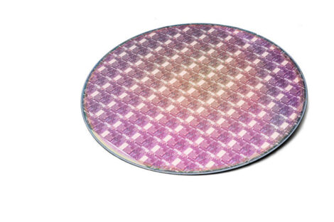
One obvious technique for improving photovoltaic efficiency is ensuring that the light sensitive surface of a solar cell captures as much sunlight as possible and turns it into electrical current. The PV industry has already invested significantly in reducing the width of the metallized silver conductor grid that is screen printed onto the front side of the cell to harness the current but which effectively shadows the precious light-capturing capacity beneath. However, current feature-widths stand at 100 to 120 µm, meaning that the shadow effect has been reduced as much as possible through existing PV process production.
Finer line work does not provide a solution either, since the finer the line, the lower its cross-section profile due to print paste rheology and the physical properties of printing screens and the higher its impedance to current flow. The solution has increasingly emerged in the form of PoP, an advanced process designed to give finer grid lines more height. By printing the lines twice over or more, PoP increases the conductor’s cross-sectional area to enhance current-carrying capacity without shadowing more of the underlying silicon substrate.
While PoP delivers an obvious solution to solar manufacturers’ efficiency dilemma, it will only be successful if print platform technology delivers nothing less than repeatable accuracy – a fundamental enabler for this process. To illustrate why repeatable accuracy is critical here, let’s use a simple analogy. In archery, if you shoot at a target and all your arrows fall within a five inch circle, but near the edge of the target face, you’ve got repeatability but not accuracy. But if you adjust your sight and hit the centre gold every time, you’ve got accuracy and repeatability – a perfect performance.
Believe it or not, the same applies to printing silicon solar cells. If you are printing one pattern, it probably won’t matter if it’s out by a few microns. But, if after metallization, you put the same cell through again and want to print on top to build conductor height, you must be both accurate and repeatable. If not, you risk your yield and ultimately, your productivity. To take another analogy, you can imagine the need for PoP to be similar to constructing tall buildings in city centres; you cannot afford to build real estate low and flat to accommodate everybody, so you build high instead. Each subsequent print pass is, in effect, like adding a new storey on top of the previous one. Obviously, you must build accurately as the floor cannot be hanging over the edge of the storey below! And it’s not enough to be accurate; you must be accurate every time since alignment accuracies must fall within an exacting 10 µm. The situation has clear implications for the screen printing technologies used in metallization.
Next-generation technologies
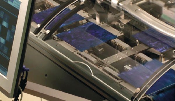
Screen printing is the optimum process to deliver metallization. It is the process of choice for all progressive solar cell producers; a precision science deployed in a wide range of innovative industrial applications from product labels to embedded passive electronic components and conductive inks. Thanks to the synergies present between other market sectors and solar cell processing, pioneering screen printing vendors are driving accuracy and repeatability capabilities well beyond that normally required by solar cell manufacturers. DEK, for example, has a successful track record in the semiconductor packaging industry, and is able to produce precision miniature interconnects for chip-scale packages using advanced screen printing technologies. Contemporary leading-edge equipment is easily capable of meeting the accuracy and repeatability requirements to produce PV cells at high yield rates. However, to meet the requirements of advanced processes such as PoP, the photovoltaic industry is demanding an even higher level of functionality.
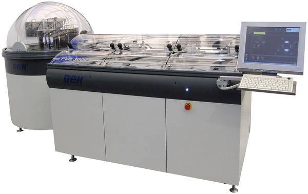
DEK Solar is one manufacturer who has answered the industry’s call, most recently with the launch of its PV3000 metallization solution. Delivering six-sigma repeatability for capability in advance of current solar cell requirements, the platform’s inherent accuracy and repeatability is ideal for demanding techniques such as PoP. Indeed, with these processes fast-becoming industry standard, the system achieves PoP capability to ± 12.5 microns at 2 cpk. The PV3000 deploys patented multiple print heads operating in parallel; if one head halts for operator attention, the others continue to print – virtually eliminating downtime – and features dedicated handling for thin wafers to ensure low breakage rates for maximum yield, as well as high-speed machine vision for perfect alignment. With print speeds up to 600 mm/sec, the metallization solution guarantees exceptional output while unprecedented handling minimises breakages.
An expanding horizon
PoP enabled by advanced platforms is finding application throughout the photovoltaic metallization process. For example, PoP capability also comes into its own in the selective etching cell structuring technique whereby an etchant is screen printed onto the cell’s surface in a grid pattern identical to that of the conductor grid. Upon heat activation, the etchant removes the cell’s top layer and exposes the silicon underneath, so that in the next print pass, the silver grid enters into direct contact with the cell’s active energy-transforming layer.
In similar vein, the selective emitter process aims to increase efficiencies by printing extra n-type dopant in a pattern mirroring that of the collection grid. The fact that the two patterns must be aligned to one other to within 10 to 12 µm is complicated by the fact that the dopant is invisible. This precludes the use of conventional vision systems, so two small fiducials, to which the two deposition processes must be precisely aligned, are typically etched on the edge of the cell. With growing emphasis on these new PoP processes it is clear that repeatable accuracy will unlock the solar industry’s path to grid parity. And with one eye fixed firmly on the future, the team at DEK Solar is committed to shortening that path for customers around the world.
ZUSAMMENFASSUNG
DEK Solar begegnet den ständig wachsenden Anforderungen in der Photovoltaik-Industrie mit der Präsentation der PV3000, einer Metallisierungslösung mit hohem Durchsatz zur Herstellung von Solarzellen. Dank der Genauigkeit und innovativen Features ist das System für anspruchsvolle Technologien bestens geeignet.
DEK Solar répond aux exigences croissantes de l’industrie photovoltaïque en présentant la PV3000, une solution de métallisation à rendement élevé pour la fabrication de cellules photovoltaïques. Grâce à sa précision et à ses fonctionnalités innovantes, ce système est parfaitement adapté aux technologies les plus exigeantes.
Share:


