For a cost-critical consumer application, we put in a multi-chip package (MCP) an ASIC plus a 1Mbit flash. We explored five substrate types comprising bismaleimide triazine (BT) laminate, high-temperature co-fired ceramic (HTCC), low-temperature co-fired ceramic (LTCC), as well as two thinfilm-on-silicon substrates. We used samples for performance and reliability tests, and they showed sufficient reliability. The substrate sizes varied quite a bit, but costs did not, because the more expensive a substrate per square, the smaller the design.
Georg Meyer-Berg and Desmond Chin, Infineon; Sven-Tuve Persson, Strand Interconnect; Albert Achen, Dow Germany
The optimum solution (defined by overall cost and manufacturability) combined latest IC and substrate technology implemented in a PSDIP-52 with leadframe. Thinfilm substrates on 200mm wafer fitted best to a standard assembly process. We successfully qualified a thinfilm aluminum/BCB (benzo cyclo butene) substrate technology from Strand. Moreover, we had to develop a special fine-pitch Au wire-bonding process.
Matching MCM requirements
The dogma that a single-chip system solution is always the cheapest is not valid anymore. A very close and broad view of the total cost is necessary. Economics are not always the only driver. What forces for building MCM exist? It can all be boiled down to three arguments: MCMs lower the size, increase the performance and may lower the cost.
Each of these benefits can be reason enough for an MCM. It can achieve all these advantages at the same time because they are interrelated. The most widely accepted argument is that an MCM or its subtypes such as multi-chip package (MCP), system-in-a-package (SiP) and few-chip module (FCM) lower the system size. This is achieved by putting the dies in one package. Further, this allows smaller boards that are enhanced by a lower interconnect density. This reduced size has direct consequences on increased performance. Due to high density or application-specific substrates, the shielding and frequency domain can be optimized, too. This can be an enabling technolgy, e.g. when signals are very weak.
In recent years, MCMs did not pay-off because of high cost for known-good-die (KGD), high costs for substrate and assembly, including low yields. The lower cost for GED (good-enough-die) instead of KGD, the progress in substrate development and thus reduced assembly expenses lowered the MCM cost overhead significantly. As a rule of thumb, a high pin count ( >400) system based on one device is cheaper as an MCM, because one high-density BGA, even with two dies, is cheaper than two. But development cost can eat up all the advantage of a single chip if one can instead reuse one or more dies in a low-volume MCM business. Also, wafer yield loss on a big single die ( >100 sqmm) can be so expensive that savings on a multi-die scenario are bigger than the MCM overhead cost.
Choice of construction and material
The mixed-signal ASIC (figure 1) is a microprocessor with up to 128 kbyte internal ROM. Provided with firmware in the ROM, the single-chip solution has an identical functionality which the MCP hasn’t. It instead has its firmware stored in an internal flash. During ramp up, as software development takes much time (time-to-market is critical), a few months of regular production time after firmware completion for a single-chip device is a problem. However, the MCP is available instantly. Furthermore, for smaller volumes, the IC ROM mask cost does not pay off. Other requirements have been the P-SDIP-52 package. Additionally, customers have not wanted to spend effort and space for a board using an external flash for the same purpose, resulting in the final decision for this MCP.
This device concept was the starting point for the MCP. Many vendors provide non-volatile memories, and very many do supply substrates. How can one find an optimal solution? Where is the assembly service for a challenging, but extremely cost-sensitive production? The only initial requirements have been that the final product has to pass Infineon’s standard consumer qualification, and that the overall cost for high-volume production should be minimal. Our approach was first taking care independently of assembly and dies, and finally to opt for the substrate, as this selection depends on the previous steps.
For the assembly, we used one of our subcons. We have gone for best pricing and quality. For the flash, five different die sources were evaluated on the following criteria: price, geometrical size, delivery forms, availability and maturity or known-good-die (KGD). Only two sources passed selection which were evaluated by building MCP samples. The flash from SSTwas superior in quality, maturity, pricing and size. This supplier uses a patented concept, leading to lower sizes and production cost than other solutions. A further advantage is the improved testability, because the erase cycle is an order of magnitude faster than others. This enables write, read and erase tests on standard automated test equipment.
Substrate selection
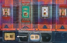
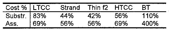
The challenge in substrate selection is not only in finding a vendor, but to determine the optimal technology. Major choices are laminates, HTCC and LTCC and thinfilm substrates. Each of these had a fixed pricing assigned to it: from cheap laminates to expensive thinfilm. However, this is only true for the substrate price per area/layer, but the real overall costs are different. We evaluated five different technologies. All had to deliver 200 bond pads, 100 nets and their shielding. All substrate designs have been used for MCP sample manufacture (figure 2 with the unmolded items). The samples in clockwise order, starting at top left, are the Strand Al/BCB thinfilm substrate, followed by the BT, the HTCC, the second Cu/BCB thinfilm and the LTCC (also shown within the open SDIP-52). It is obvious that the size of the substrates varied by factors. The HTCC used four metal layers, the LTCC three, and all others were based on two layers. Consequently, the total price for the substrate was the lowest for both thinfilms. Only the laminate type could have competed in pricing, but the quote could not.
How did the substrates influence assembly and thus add further costs? The thinfilm substrates were ideal in handling as they are supplied in wafer form. This is more effective than picking from trays as with the other substrates. Furthermore, the laminates had the drawback of requiring plasma cleaning before assembly. Finally, the pad position accuracy was not good for ceramics, better for laminates and superior for thinfilm. This not only leads to a smaller design, but also to fewer stops during wire bonding.
Aluminum/BCB thinfilm on silicon substrate
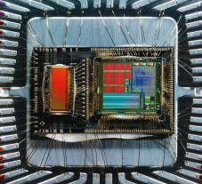
Another difference of the MCP solutions is the time-to-production for the substrate assembly tooling. For thinfilm, it took only a week to get the production tools, for laminates it took a month, and for ceramic it was three months. All versions passed a standard package qualification. Tests included a 96h pressure-cooking (100% humidity/121°C), up to 1000h temperature storage at 150°C, and up to 1000 temperature cycles from -40 to +125°C. At physical analysis, no sample showed any weak-ness. Because all solutions fulfilled these requirements, we were free to choose the cheapest. The final construction was based on a chip carrier from Strand, as seen in figure 3.
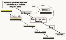
The qualified process for the substrate is a thinfilm aluminum/ photo-BCB process on 200mm wafers. Several interconnect layers made of sputtered aluminum with a thickness between 1 to 3µm can be built up (figure 4). Where controlled impedance or good power decoupling is required, power and ground planes are added into the thinfilm structure. The dielectric layers consist of a 3 to 7µm thick photo-definable polymer dielectric. The dielectric is based on the widely used low-k benzo cyclo butene (BCB) dielectric from Dow Chemical. This dielectric is manufactured in both dry-etch and photo-definable formulations that are prepared as ready-to-use solution for spincoaters. Main electrical advantages are the low loss and low dielectric permittivity, both of which are being stable up into the THz range.
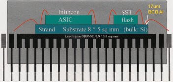
All processing is done in an automated 200mm wafer line. Production takes place in a class 10 to 1000 cleanroom. Wet processing (cleaning, developing, etching) is run in automated batch mode to minimize handling of individual wafers. The process flow is controlled, giving full traceability of materials and process steps. The major steps are spincoating of the dielectric (figure 5), sputtering for the metal interconnect, proximity exposure, immersion development, wet/plasma etching and curing. Measuring several test structures on each wafer continuously monitors the process. Production yield has been found to be mainly exposure mask age-dependent. The substrates are individually marked with their wafer position giving enhanced traceability. All substrates are 100% open/short tested, and supplied in wafer form. The process is stable and reproducible over long periods. Although this is a sensitive mixed-signal design where several nets require special consideration regarding cross talk and shielding, two layers of 3µm aluminum were found sufficient to handle both signal and power routing. The minimum design rules were 20/25µm line and spacing with 30µm vias and a minimum pad pitch of 125µm. The substrate contains 100 nets and 165 vias, and its size is 8 x 5mm. The testability issue taken into account was that a single probe card should reach all bond pads.
Assembly development
The MCP assembly was classified intotwo categories: low-cost strategy and the introduction of Strand material. To align with this aim, standard materials and assembly equipment have to be utilized as much as possible. Due to assembly viability and cost competitiveness, thinfilm substrates on 200mm silicon wafer were selected, although the constraints from this technology were not yet fully understood with respect to packaging and re-liability. The 200mm platform was con-sidered because infrastructure well exists for the backgrind, mount and saw operations.
To accommodate the substrate on open tool leadframe (area 8.89sqmm), the substrate size has to be smaller, but big enough to accommodate both the ASIC and the flash. Therefore, a smaller substrate design becomes critical to die attach. Glue thickness (underneath ASIC and flash), glue coverage, placement accuracy (first for substrate, second for both ASIC and flash), and planarity of substrate and dies are all influential variables. They must be controlled within specification since there is a direct correlation to package and product reliability.
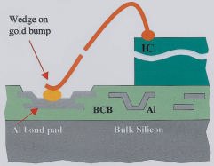
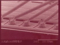
The bond pad structure is Al build-up, and the surface consists of 99.5%Al/0.5%Cu. If the wedge is applied directly onto Al bond pad, either a broken wedge or a damaged pad is observed. The frequency was very high, resulting in machine halt for every bonded wire. After evaluation, we deduced that the bond pad structure is not rigid enough for wedges. So, a wedge-on-bump concept was considered. For this, a gold bump is first bonded onto thepad, after ball bond on IC, the wedge is then bonded onto this bump (figure 4 and 6). The bump presence cushions the wedge force from damaging the Al bond pad. During bumping, lifted metal (destructive) and non-stick (reworkable) failures do occur occasionally, but frequen-cy was greatly reduced after optimization. The process yield was significantly improved. With the introduction of 140 bumps (takes additional 45s), the throughput was reduced by 40%, and assembly cycle time was longer, but significant benefits were gained from high assembly yield and productivity.
Qualification and ramp-up
To achieve good yield, we do not only need a stable assembly process, but a stable component process as well. The substrate yield has improved to 98%, and the flash yield is not much worse. We achieved assembly yields better than 98% and backend test yield of 98%. The MCP passed the standard qualification based on 77 samples per test, done with additional ESD and latch-up checks.
When working samples of all versions were available, they were tested in the application, and underwent performance verification. These were analog measurements of noise, sensitivity, filter and group delays. All versions showed same results within defined accuracy. The results were as good as with a single-chip version. As all the analog performance comes from the IC, the MCP could achieve the same performance as maximum.
The cost base for MCP assembly is the expense for the single-chip. Main adders are the costs for the flash and for the substrate. More complex cost adders for the MCP versus the single-chip assembly are the substrate attach, the second die attach and the 130 additional bond wires (see small table). Further expenses come from the test time (0.2s) for the flash, the yield losses from flash and substrate, and the more difficult assembly. We counted the yield losses caused by the IC, because in the single-chip version, the loss is just the package. The difference in the thinfilm solutions was minor, and we have chosen the Strand substrate for reasons of volume availability.
As more and more IOs are needed per chip area, the routing density supplied by the substrate is more important than just looking at the price. As the integration of passives in thinfilm technology will become more important, such a substrate in high-performance application is the cheapest solution. The supply and demand for the product was partly fifty times the planning, and all the ramp-up happened without yield loss. So far, Si/BCB/Al substrates have not been used in molded plastic packaging before.
Condensed version of a paper presented at the International Conference on High-Density Interconnect and Sys-tems Packaging 2001, Santa Clara. Used with kind permission of IMAPS.
References
Jan Carlson: 486 Computer Module System. Proceedings of 1995 International Conference on Multi-Chip Modules, Denver, Colorado
Strandberg, Thiede, Karlsson, Weiland: High Reliability 4 Metal Layer MCM-D Structure with BCB as Dielectric. Proceedings of 1995 International Conference on Multi-Chip Modules, Denver, Colorado
Eric Chieh, Philip Garrou, R. H. Heistand, Chung Ho, Jim Lykins, Brian Martin, Timothy Rehg: Thin Film Polymeric Materials in Microelectronic Packaging and Interconnect. Proceed. Int. Symp. Adv. Packaging Materials, Atlanta, 1998
H. M. Heiliger, M. Nagel, H. G. Roskos, H. Kurz, F. Schnieder, W. Heinrich, R. Hey, K. Ploog: Low-dispersion thin-film microstrip lines with cyclotene (benzocyclobutene) as dielectric medium. Appl. Phys. Letters 70, 1997
M. Nagel, C. Meyer, H.-M. Heiliger, T. Dekorsy, H. Kurz, R. Hey, K. Ploog: Optical second-harmonic probe for ultra-high frequency on-chip interconnects with benzocyclobutene. Appl. Phys. Letters. 72, 1998
P. Garrou: Wafer Level Chip Scale Packaging: An Overview. IEEE Trans. Adv. Packaging, Vol. 23, 2000
Zusammenfassung
Für eine hochvolumige Consumer-Anwendung wurde ein MCP (Multi-Chip-Package) mit einem Prozessor und einem Flashspeicher realisiert. Die Single-Chip-Lösung wurde grundsätzlich verworfen. Als kostengünstigste Alternative unter fünf MCP-Mustern stellte sich der Aufbau als Dünnfilm-Substrat auf Silizium heraus. Weil das Substrat in Waferform (200 mm) zur Verfügung steht, wurde die Fertigung auch auf solch einer Linie durchgeführt.
Résumé
Un MCP (Multi-Chip-Package) destiné aux applications volumineuses a été réalisé avec un processeur et une mémoire flash. La solution „single-chip“ a été rejetée par principe. La réalisation d’un substrat en film fin sur silicium s’est avérée être une solution économique. Comme le substrat est disponible sous forme de tranche (200 mm), la fabrication a été réalisée sur une telle ligne.
Sommario
Per l’uso da parte di una grande massa di utilizzatori é stato realizzato un MCP (Multi-Chip-Package) dotato di un processore e di una memoria piatta. La soluzione Single-Chip é stata fondamentalmente rifiutata. Fra i cinque campioni MCP, la soluzione più economica si é rivelata quella caratterizzata da un substrato in pellicola sottile su silicio. Poiché questo substrato é disponibile come wafer (200 mm), anche la produzione é stata eseguita su una tale linea.
Share:


