A digital detector lowers the threshold for contrast detection, to allow X-ray imaging of non-conductive die-attach for the first time. Such a detector is easier to operate, since its image quality does not depend as strongly on X-ray parameters as that of an image intensifier. Laminography is of advantage wherever 3D-information cannot be provided by oblique 2D views as it is with flat objects (PCBs, layers, etc.). Now, by OVHM technique (oblique view at highest magnification), object tilting can be avoided, and therefore, sufficient magnification can be easily adjusted in oblique view.
Holger Roth, Phoenix X-ray Systems + Services
Wilhelm Conrad Röntgen, discoverer of radiation and after whom X-rays in German („Röntgenbilder“) were named, realized its benefits for non-destructive testing. In his publication „Über eine neue Art von Strahlen“ (About a new kind of rays), he mentioned a photograph of a piece of metal, „the inhomogenity of which becomes noticeable through the X-rays“. The explanation of the radiation mechanism immediately led to the conclusion that the resolution or sharpness of the images could be improved by reducing the size of the X-ray source, which means by reducing the diameter of the focal spot of the electron beam on the anode. However, the electron-optical instruments such as lenses, etc., necessary to achieve this in an effective way, had still not been invented at this early time.
In 1951 V.E. Cosslett und W.C. Nixon (Cambridge) reported of an „X-ray shadow-microscope“, which they had constructed utilizing a magnetic electron-lens as proposed earlier by Manfred von Ardenne. Another two decades later, this technique found its first industrial applications when micrometer scale defects became an issue due to miniaturization of electronic devices and assemblies as well as increased reliability requirements.
Fundamentals of technology
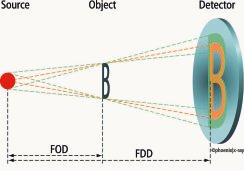
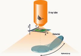
In a microfocus X-ray inspection system, the specimen is irradiated by a cone-shaped beam. It generates a magnified image on a detector which , in most cases, is still an image intensifier. The detectabilty of structures or details through an X-ray image is ruled by three properties: magnification, resolution and contrast.
The resolution (image sharpness) of a system is mainly determined by the size of the X-ray source which is in the range of a few microns for microfocus X-ray tubes. The geometric magnification is given by the geometry of the beam (illustrated in figure 1), and can be as high as 1000x to 2500x at practicable distances. Apart from resolution and magnification, the recognition of an individual object feature depends on the contrast induced by this detail to the image. Physically, the contrast originates from different X-ray absorption properties of different object areas, and can be caused by varying thickness (e.g. shape of a solder joint), as well as by different materials such as copper conductors on a printed circuit board (see figure 2).
The detectabilty of a given contrast is technically limited by the detector properties. For the image intensifier, as a rule of thumb, we may say that the absorption difference must amount to at least 2% to be detected in the X-ray image. For a contrast solely caused by varying thickness, in first approximation a linear relation to the absorption difference can be assumed so that the difference in thickness must also exceed 2% of the total thickness to be visible in the image.
New challenges to X-ray technology arise when novel objects, details or defects are to be displayed which, due to their size or material characteristics, cross the described limits of contrast or spatial resolution. Therefore, for objects of very low contrast, mainly the detector technique (including software) has to be reconsidered, whereas for the detection of smaller details the X-ray tube design is of interest. Furthermore, increasingly three-dimensional information on the object is required.
Low contrasting objects
Take, for example, non-conductive die attach. The adhesive mainly consists of low-absorbing elements (N, O, H, C) and can be concealed in the X-ray image already by a thin copper layer in the substrate (see figure 3). Another example are extended solder die-bonds on thick copper or tungsten-alloy heat sinks. Here, the solder layer shows strong absorption, but is very thin compared to the heat sink. Then we have multilayers with many or extremely thick copper layers: a single copper layer is very thin in relation to the sum of the others and, hence, only yields insufficient image contrast. In addition, in case of micro-mechanical devices, the microscopic structures have to be detected in light materials of low absorption.
For all those applications, recently a digital detector has been launched which not only shifts the detection limit for contrast differences from 2 to 0.5%, but also provides a live image of several frames each second. Furthermore, this detector, due to its pixel set-up and its high dynamics (65,000 gray values), is quite insensitive to oversaturation effects. This is in particular an advantage for the inspection of objects with strong absorption differences such as castings. However, just because of the high dynamics, the desired image information is enclosed in a relatively narrow gray-value range that the human eye cannot differentiate. Dedicated image processing software filters out the gray-value range of interest in real-time, displaying it in an appropriate way, making it accessible to the proven automatic evaluation procedures such as the measurement of annular ring widths in PCBs and the voiding analysis of die-attach. This detector-software set yields good results, and also in many cases the image quality turns out to be less dependent on the tube parameters, making the detector easier to use than an image intensifier, for example.
Very small object features
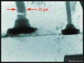
There are many examples for features that have to be detected in very small objects. For example, in microvias the hole diameters may be as small as 25µm, and possible irregularities can be even much smaller. For the verification of bonded wires, the wires typically measure 25µm in diameter. Defects such as breaks or cracks have to be detected in the micrometer and sub-micrometer range (see figure 4). And in case of flip-chip solder joints, pitches of 50µm and less are now achieved.
As opposed to low-geometric magnification (1x to 10x) at which the detector resolution also has an influence, at high magnifications almost exclusively, the size of the actual X-ray source determines the spatial resolution. Just some months ago, also in this field, a breakthrough was achieved. Now a nanofocus X-ray tube for industrial application is available. It features a source size of remarkably less than 1µm that can provide a detail detectabilty of less than 500nm (0.5µm) at 1000x to 2500x geometric magnification. Not only defects of this size can be detected, but also any high-magnification inspection becomes easier because of better image definition.
Three-dimensional image information
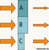
In interconnection technology, 3D information is required, so for BGAs, CSPs, flip chips, etc. The solder connections between board and substrate, respectively, and the dies have to be inspected separately. Not all open solder joints can be detected in top-down view. For through-hole plating, the metallization is to be inspectedfor integrity, and for measuring purposes. Moreover, in the case of stacked-die components, where normally two or three dies are arranged above each other in a single configuration, adhesive or solder layers have to be separated in the image.
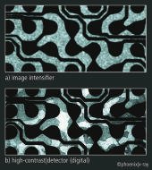
In the beginning, laminography appeared to promise a solution for all those inspection tasks, but it turned out that a more flexible approach is necessary. Laminography delivers good results in case of planar objects such as PCB/substrate layers or adhesive and solder deposits, but for objects which continuously extend in the third dimension, image interpretation is quite difficult. Picture artifacts that are characteristic for the presently available laminography technology affect the layer images. Practice shows that the detection efficiency of laminography is not very high for open solder joints: the gap in the joint can only be identified among the image artifacts if it is sufficiently wide.
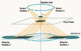
For example, a laminography image (figure 5) is recorded while the specimen is irradiated under an angle J, and detector and X-ray source are moved synchronously on circular paths as illustrated in figure 1. The points of the so-called focus plane, the object plane that includes the intersection point of rotational and X-ray beam axes are always imaged onto the same points of the detector surface. The images of object points outside the focus plane move on the detector in circle paths during the rotation of detector and source. With an integrating detector (radiographic film), a sharp image of the focus plane is obtained which is superimposed by blurred contributions of out-of-plane objects. Now, the object might be shifted through the focus plane, and in this way be imaged layer by layer. For each layer, a rotation by 360° (acquisition cycle) is required.
In digital laminography (similar to computer tomography), single projections are digitally recorded at fixed positions during a single acquisition cycle. From these projections, many object layer images can subsequently be reconstructed by means of numerical algorithms. In the simplest case, the object shift is simulated by superimposing and averaging the projections. In particular, the direct average of the projections again gives the layer image corresponding to the focus plane. Furthermore, based on the layer images, three-dimensional visualization of distinct object areas can be generated, which then can be looked over from all directions on the screen. The integrating method requires 1 to 2s to display a single-layer image. In digital laminography, 8 to 100 projections are recorded within 1 to 15 minutes, the evaluation of which again takes from a few seconds to 20 minutes, depending on the algorithm. Providing that the data is suitably processed, the digital method in general yields a higher image quality than integrating.
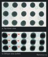
A study has lead to the conclusion that X-ray inspection in oblique views yields the highest detection probability for open solder joints. However, using the customary system set-up for the inspection of smaller solder joints (FBGAs, CSPs, BGAs and flip chips), no sufficient magnification could be achieved in oblique view due to the increase of the distance between object and X-ray source after tilting the object. Now, by means of the OVHM technique (oblique view at highest magnification), object tilting can be avoided so that a sufficient magnification can be easily adjusted (figure 6) as well. Figure 7b displays such an OVHM image of the fifteen solder joints which are shown in a top-down view in Figure 7a. Evidently, the liquid solder did not wet six board pads which are not connected (open). The OVHM technique reveals immediately defects(an image is generated within just a second)that are hidden by artifacts in laminography. It is a powerful and efficient method to detect wetting defects in solder joints of area-array pack-ages.
ZUSAMMENFASSUNG
Mit der fortlaufenden Entwicklung in Advanced-Packaging und Miniaturisierung ist es nötig, innerhalb von Substraten, Leierplatten oder Komponenten im Rahmen der Qualitätssicherung mögliche Defekte zu lokalisieren. Die Röntgentechnik nimmt dadurch weiterhin eine rasante Entwicklung, sei es durch Röhren mit Nanometer-Auflösung oder weiter verbesserte Methoden wie OVHM (oblique view at highest magnification).
RÉSUMÉ
Dans le cadre de l’évolution ininterrompue des Advanced-Packaging et de la miniaturisation, il est nécessaire de localiser les défauts possibles, au niveau de l’assurance qualité, dans les substrats, les cartes imprimées ou les composants. Ceci explique en partie le développement rapide de la technique des rayons X, que ce soit avec les tubes dont la résolution atteint le nanomètre ou les méthodes améliorées comme l’OVHM (oblique view at highest magnification).
SOMMARIO
In seguito alla progressiva evoluzione nell’Advanced-Packaging e alla miniaturizzazione è necessario localizzare tempestivamente i probabili difetti all’interno di substrati, circuiti stampati oppure componenti nell’ambito della sicurezza della qualità. La tecnica radiogena in tal modo assume un ruolo sempre più importante nell’ambito della sua rapidissima evoluzione, sia attraverso tubi di risoluzione nanometrica che tramite altri metodi ancora migliori, quali ad esempio OVHM (oblique view at highest magnification).
Share:


