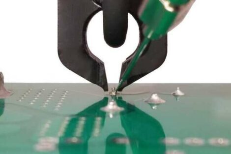
In recent years, the production of RoHS compliant components has resulted in one of the most expansive material changeovers in the history of electronics. In particular for the utilized components, higher soldering temperatures cause additional stressing. Moisture sensitive IC packages and electrolytic capacitors are affected to an especially great extent.
Dr. Hans Bell and F. Oswald, Rehm Thermal Systems, R. Heinze and Dr.-Ing. H. Wohlrabe, TU Dresden, J. Pfülb, Beck, H. Yamada and T. Nakamura, ELNA
As yet, there are no standards for the component manufacturers which define reflow soldering in terms of practical temperature-time limits. Only the specifications provided by the respective suppliers are available for the group of components consisting of electrolytic capacitors, which often do not take essential manufacturing conditions into consideration. Additional knowledge is thus absolutely essential for the production of reliable components. The first part of this presentation introduces the results of several examinations regarding the thermal stability of a number of IC packages and electrolytic capacitors during the soldering process, and addresses the effects of interaction amongst various influencing factors on soldering results.
Moisture sensitive components
Various packages rated MSL 3 and 4 were used for examining moisture sensitive ICs, namely SOT, SSOP, PQFP, MQFP and PFCM. All of the examined ICs were removed from their moisture resistant packages before soldering, and were placed into storage for 72 or 168 hours at a temperature of 30° C and a relative humidity of 60% in accordance with their moisture sensitive levels (MSL). The components were then subjected to different reflow stressing variants as shown in the table. Both before and after respective thermal stressing, the ICs were examined with an ultrasonic microscope using the pulse-echo technique (C-scan).
Due to the fact that the transferred heat originates from phase change enthalpy (gaseous to liquid), 10 to 20 times more heat is transferred during the same period of time by means of this reflow process than with convection soldering, which works with hot nitrogen or hot air. Damaged components, for example delamination, are thus more likely with condensation soldering. Vacuum represents an additional stressing factor for moisture sensitive components. Residual moisture considerably increases internal pressure inside the package during reflow soldering, and the vacuum increases the relative pressure difference by an additional 1 bar. This is why emphasis was placed upon vacuum condensation soldering in our study. Subjecting the components to stressing three times was intended to demonstrate the ruggedness of the components, even in the case of multiple soldering. Maximum temperature was set to 260° C for convection stressing. This corresponds to the maximum temperature rating for moisture sensitive components in accordance with the JSTD IPC 20C standard. The condensation soldering system was filled with Galden HS240, which means that the maximum temperature for this process did not exceed 240° C. During the course of adaptive vacuum stressing, a final pressure of <10 mbar was achieved for a period of approximately 30 seconds. The heat gradients were always <3 K/s. All of the components available to us had a moisture sensitive level of MSL3, except for one component which was rated MSL4 (in accordance with IPC 020C).
The examined SSOP and SOT components have very rugged packages, which didn’t demonstrate any delamination even after being subjected to reflow stressing several times. The MQFP80 and MQFP144 packages proved every bit as rugged as well. As opposed to this, the PQFP64 already demonstrated slight delamination after convection soldering, as well as after convection soldering without vacuum, although the bottom of the chip carrier did not demonstrate any changes at all. Delamination at the chip carrier/mold compound level increases as soldering stress becomes greater, and spreads out over the entire surface of the pad. 90 % of all tested PQFP64 packages failed after being subjected to vacuum condensation soldering twice.
Sensitivity to reflow stressing also increases with more complex package designs, which has been substantiated, for example, by means of the examined PFCM128. The chips on the ICs are bonded to interposers, which in turn are mounted on the middle pad of the leadframe. Delamination at the interposer/leadframe level becomes apparent to an ever greater extent as reflow stressing increases.
Convection soldering demonstrates defect patterns which are similar to those of condensation soldering without vacuum. Minimal or no changes at all can be substantiated in the packages which were subjected to thermal stressing one time only. More complex packages may be destroyed when subjected to reflow stressing several times with vacuum. With regard to thermal stability during the soldering process, no difference between the PFCM100 with a moisture sensitive level of MSL4 and a PFCM128 of comparable design with a moisture sensitive level of MSL3 occured. Thus thermal stability during the soldering process is not characterized by the degree of sensitivity to moisture.
Capacitance loss of electrolytic caps
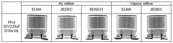
The following package types were used for examining thermal stability during the soldering process: D10x10L, D8x6.5L and D6.3×5.3. For these components, thermal stressing during reflow soldering was based upon the IPC J-STD 20C and IEC 60068–2–58 standards, as well as the ELNA specification. Due to the fact that electrolytic capacitors are also frequently exposed to the condensation soldering process, stressing under vapor phase as well as convection reflow conditions was carried out. The electrolytic capacitors were not specified for the vapor phase process. All of the process parameters were adjusted such that allowable temperatures in accordance with the standards were not exceeded. All of the electrolytic capacitors were examined by means of X-ray for possible mechanical defects after thermal stressing, and electrically measured. No mechanical defects could be detected at the capacitors after either convection soldering or condensation soldering.
The electrical measurements revealed capacitance losses after each reflow process in all cases. Considerably greater thermal transfer in the case of vapor phase soldering also resulted in larger capacitance losses for all examined types of electrolytic capacitors. Several capacitors were subjected to stressing two and three times in the same convection reflow process. Subsequent measurements revealed that capacitance loss is further increased. When exposed to thermal stressing three times using the convection process, the same amount of capacitance loss occurs as is also the case after exposure to stressing only once with the condensation process.
Effects of reflow params on soldering results
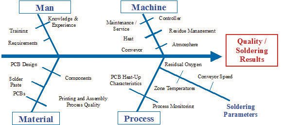
Numerous influencing factors effect the final quality of a PCB, some of which are depicted as an Ishikawa diagram. Due to this great variety, the user is frequently faced with the question of which combination of influencing factors results in ideal quality. During the last two years, systematic testing of reflow quality has been conducted at the Electronics Packaging Lab of the Dresden Technical University with vital support provided by Rehm Thermal Systems.
Wetting Quality: The surface of the PCB has a significant influence on wetting quality. Results of an evaluated test shows for which chemical tin demonstrates better wetting. In contrast to this, the expected results were obtained from the first test, i.e. nickel-gold demonstrated better wetting. It is generally expected that tin reacts more sensitively to oxidation. The cause of these contradictory test results can be traced back to the differing levels of quality of the utilized PCBs. The mentioned results demonstrate the complexity of the various influences on reflow quality.
Wetting quality at the chips was evaluated by means of AOI. A total of approximately 300,000 solder joints were recorded. The smaller the measured gap was, the better the wetting was. It also shows the influence of the utilized peak temperature.
At a higher peak temperature of 245° C, the gap becomes smaller. As temperature rises, chemical-metallurgical interaction increases and the surface tension of the molten solder is reduced, which promotes wetting on the whole.
Reflow Atmosphere/Nitrogen: The use of nitrogen in reflow soldering plainly has a favorable effect on wetting quality. During testing, residual oxygen content was varied from 100 to 1000 ppm instead of soldering in normal air. Nitrogen displaces atmospheric oxygen in the reflow atmosphere, and thus prevents oxidation of the surfaces to be wetted.
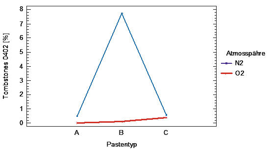
Tombstones: However, interactive influencing factors may lead to different quality results. For example, the number of tombstones rises as conveyor speed is increased in a nitrogen atmosphere, whereas it remains nearly constant in an air atmosphere. Oxidation processes acting upon the surfaces to be wetted and the solder paste in an air atmosphere increase wetting time and thus reduce delay time between the right and left connectors. Pastes with adequately good wetting characteristics are also capable of achieving equally low numbers of tombstones in a nitrogen atmosphere as is also the case in air.
Whereas a nitrogen atmosphere may promote the occurrence of tombstones, it has a positive overall effect on wetting. With the help of nitrogen control, by means of which the selected residual oxygen level is held constant, and additional setting parameter is placed at our deposal for counteracting tombstones.
Solder Balls: Solder balls at the 0805 and 1206 chips were counted by means of AOI. The primary influencing factor for beading is the solder paste’s grain size. The smaller the grain diameter, the more probable it becomes that grains will be displaced into the gap underneath the chip component. Due to the larger overall surface area of the metal contained in the fine grained solder paste, oxidation with residual oxygen also occurs to a greater extent, and beading is thus promoted. A higher peak temperature reduces the molten solder’s surface tension, and the solder is thus even more easily forced into the gap.
Furthermore, the chips drop down further during the soldering process when a higher peak temperature is used, which is confirmed by the stand off measurements. The size of the gap underneath the component is thus reduced, which enhances the capillary effect. Longer preheating times minimize beading. They promote more thorough drying out of the solder paste, thus reducing the flow of liquid (flux) underneath the component and the number of solder grains which can be displaced.
Voids: Void analyses were conducted at BGA and surface solder joints (QFN, Si chips). Test evaluation resulted in obvious contradictions. Ball and surface solder joints necessitate different reflow settings in order to achieve minimal void content (except for the solder paste’s grain size).
Only a small number of voids occur at the BGA with poor wetting quality. The reverse is true for the QFN: good wetting quality also results in a small number of voids. Solder paste grain size is here the exception. Furthermore, for both the BGA and the QFN, peak temperature has a greater influence on voids.
For the QFN package, a higher peak temperature also results in a longer dwell time for the solder in its molten state, which means that gas bubbles have more time to escape. The viscosity of the molten solder is also reduced at higher temperatures, which also facilitates the escape of gas bubbles. In the case of the BGA, delayed wetting due to poorer wetting characteristics could facilitate the escape of gas bubbles. An oxide layer is formed on the surface of the molten balls due to the higher peak temperature, which impairs further escape of gas bubbles.
If both types of components need to be soldered to the same PCB, there are no ideal settings which are capable of minimizing all voids – neither with regard to the utilized materials, nor concerning reflow parameters. The primary causes of contradictory performance are initially to be discovered in the geometric differences of the various components. A significant reduction in the number of voids can only be achieved with the help of vacuum soldering processes.
EPPE 410
zusammenfassung
Die Herstellung von RoHS-konformen Baugruppen hat in den letzten Jahren zu einer immensen Materialumstellung geführt. Betroffen sind besonders die Bauelemente, deren Stressfaktor durch die höheren Löttemperaturen gewachsen ist. Für den Baugruppenfertiger gibt es noch keine Standards, die das Reflowlöten in sinnvollen Temperatur-Zeitgrenzen beschreiben. Daher sind zusätzliche Kenntnisse für die Herstellung zuverlässiger Baugruppen notwendig.
Durant ces dernières années, la production de composants conformes à la directive RoHS a entraîné des changements considérables dans le domaine des matériaux, affectant surtout les composants dont le facteur de stress en raison de la hausse des températures de brasage. Les producteurs de composants ne disposent pas encore de normes définissant les limites de temps/température adéquates pour le brasage par refusion. La production de composants fiables nécessite des connaissances supplémentaires.
Share:


