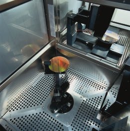
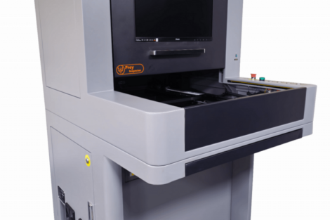
The speed of the Siscan 3D surface inspection system of Siemens Dematic has been quadrupled, to achieve a throughput of 17 wafers per hour (200mm with 110,000 bumps, XY-resolution 10µm, submicrometer Z-resolution). Based on the principle of confocal microscopy, it provides accurate measurements. Doubling the measuring channels and rising measuring frequency have achieved the increase in throughput. This has reportedly made it the world’s fastest laser verification instrument for vias, volume inspection of solder paste and adhesive, and the 3D measurements of bumps on wafers and substrates. With the integrated handler, it can process wafers from standardized cassette systems such as Foup 300mm or Open Cassette, but also film frames and thin wafers. Siscan measures heights from 10 to 400µm, XY-position and offset, coplanarity, etc.; also customized measurement parameters can be defined. Interfaces such as GEM/SECS II ensure that the results can be stored and be available at all times.
Share:


