Modern electronic products have put high requirements on the cost-effective assembly/connection technology of semiconductor (bare) chips and packaged components, respectively. In this three-part article series (published in EPP Europe issues # 9/10, 11/12 and first of 2003) we will cover the basics, engineering trends and application areas of flipped chips (forms the core of advanced packaging) as well as the requirements placed on the assembly equipment.
Hugo Pristauz, Datacon Semiconductor Equipment
The technology and application of flipped (naked) chips has reached a particular level of maturity which becomes visible, among other packaging innovations, in the advent of flip-chip solder-bump technology as the upcoming mainstream in die-substrate assembly. Parallel to this development, the industry is forced to provide high efforts in reducing package costs. With the use of cheaper flex substrates, an ongoing trend from wire bonding to flip-chip assembly based on adhesive joining technology can be seen. No-flow underfill or single-pass reflow encapsulants (SPRE) can render flip-chip technology even more attractive by cost savings. In such an application scenario of established and rapidly advancing technologies, users need reliable and flexible equipment partners who can also provide a profound kind of technology transfer.
Advantages of flip-chip assembly
The assembly of flipped chips offers convincing advantages over conventional wire bonding. Primarily, these are reduced space requirement, assembly height and weight. Apart from that, the contact pads are not confined to the periphery of the chip (as with traditional ICs), but are distributed over its entire surface, thus allowing more interconnects or a wider pin pattern. This forms a so-called field array of contacts or bumps, respectively. In addition, the shorter electrical connections lead to lower line inductances and smaller parasitic capacitances and resistances, which brings about better use of the high-frequency properties of the chips. Because the back of the chip is exposed, it can be used efficiently for heat dissipation, thus increasing the circuit performance.
Although flip-chip technology has been around for a while, for a long time it played a somewhat subordinate role. The reason for this lay primarily in the high costs. Technologies in the semiconductor industry for high-volume markets are always cost-driven, so flip-chip technology could only become established in areas where there was no cost-efficient alternative available. For example, the C4 (controlled collapsed chip connection) technology was introduced at IBM in its mainframes for high data rates, or at Delco for car electronics pertaining to the high ambient temperatures in vehicles. All this started about35 years ago.
Solder-bump flip-chip assembly
With the replacement of expensive ceramics with organic substrates, and the introduction of low-melting-point solder bumps, the opportunity for production of more cost-effective flip-chip components has been provided. However, the technical challenges were only satisfactorily overcome in the nineties; for example, the thermo-mechanical problems due to the different temperature coefficients through the availability of mechanical stress compensating underfiller material. Now, the large number of bumping services and manufacturers for microvia substrates clearly shows that the time has come for a broad application of solder bumping.
The few principle steps in flip-chip assembly are as follows: wafer bumping – wafer dicing – applying flux to the substrate – pick-up, flip, align and place chip – solder reflow – cleaning – underfill – and curing the underfill. By use of newly designed SPRE, which combines flux and underfill materials in one formulation, curing takes place during the reflow process. Therefore, the last two steps can be avoided, leading to even more cost saving.
In general, the flux is applied to the solder pads via stencil printing. Alternatively, the bumps of the chip can be dipped into a flux film before the placement. Once the chip has been placed on the substrate, the tacky flux fixes the components until the solder bumps establish the final connection during the reflow process. Then, excess flux residue must be removed, and the underfill material is dispensed on one or two sides of the chip to be sucked under the chip through a capillary effect. The concluding heat treatment cures the underfill. This protects the contacts against environmental influences, ensures a robust mechanical connection between chip and substrate, and balances out mechanical stresses through thermal coefficient mismatch to increase package reliability. Once again: using single-pass reflow encapsulant, only one dispensing and thermal processing operation will be needed.
An alternative: adhesive joining instead of soldering
For some flip-chip application there is an interesting alternative: adhesive joining. Various methods are used here: connecting with isotropically or anisotropically conductive adhesive and using non-conducting materials. The bump material is predominantly gold.
Without the danger of solder-bridge formation, smaller pitches can be implemented with adhesive technique. Furthermore, substrates can be used which cannot withstand the melting temperature of eutectic lead/tin solder (183°C) or lead-free alloys. Among others, this is the case with LC-displays; so, to no surprise, adhesive flip-chip joining has established itself for chip-on-glass (COG – mainly on the base of anisotropically conductive adhesives).
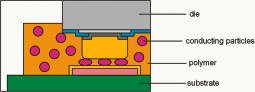
Anisotropically conductive adhesives consist of polymers, preferably in film form, which contain few conducting particles, such as nickel or gold-coated polymer balls. If the contact surfaces of chip and substrate are now pressed closer together with anisotropically conductive film between, the balls trapped between them form an electrical connection (figure 1). Under pressure and the effect of heat, the material then cures. Because these adhesive films are used over the whole device surface, there is no need for underfill.
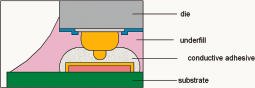
Alternatively, isotropically conductive adhesives (figure 2) can be used, such as polymers filled with small silver flakes which, like conventional solders, conduct equally well in all directions. The bonding process here is similar to that of the solder-bump process, except that, instead of flux, the conductive adhesive must be applied (stencil printing or dipping). After curing at lower temperatures than with the solder-based procedure, cleaning is no longer necessary, so the underfill process can begin immediately.
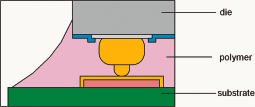
With the third variant, non-conductive adhesive is applied to the whole surface before the chip is positioned. With the shrinking of the adhesive on curing, the bumps are pressed against the pads, thus forming the conductive contact (figure 3). The omission of the subsequent underfill process leads to further cost reduction.
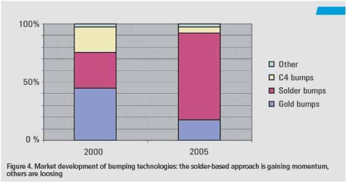
At the center of the introduction of environmentally friendly electronic products is the ban of lead-containing solder alloys. Adhesive flip-chip joining offers an interesting alternative here, although the placement process requires much higher accuracy due to the lack of the self-centering mechanism during reflow. Back in 2000, gold-bump technology, used on nearly half the approximately 4m wafers, was still predominant (figure 4), but this is set to change by 2005, with three-quarters of the 25m wafers then forecasted using solder bump technology.
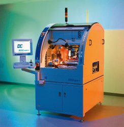
Flip-chip technology is based on a highly diverse assembly process, which can ultimately be tailored to the requirements. In the first place, it requires well-developed high-throughput equipment for established techniques, which however at the same time have to be sufficiently flexible for future technology fine-tuning. One example for such a piece of equipment is the Datacon multi-chip die-bonder 2200 apm, which offers very high precision, flexibility and compactness. Within a single machine module, chipscan be flipped, dipped in flux and aligned with extreme precision. For more sophisticated tasks or higher throughput, the platform concept allows up to four modules to be combined and fitted with the required functions. The advanced model 2200 apm+ (figure 5) processes the upcoming 300mm wafers for this promising market.
ZUSAMMENFASSUNG
Die Einführung der ersten Flip-Chip-ICs durch IBM (C4) und Delco liegt zwar bereits etwa 35 Jahre zurück, aber damals war es noch eine koststpielige Technik, die nur in einigen wenigen Anwendungen finanziell sinnvoll erschien. Inzwischen sind Field-Array-Bausteine auf der Basis von umgedrehten (flipped) Chips, die so dann auf dem Substrat montiert werden, in irgendeiner Form auf jeder modernen Baugruppe zu finden. In dieser dreiteiligen Artikelserie gehen wir auf die technischen Grundlagen und Applikation dieser populären Advanced-Packages ein.
RÉSUMÉ
L’introduction des premiers CI Flip-Chip par IBM (C4) et Delco remonte déjà à 35 ans environ mais il s’agissait à l’époque d’une technique coûteuse, financièrement intéressante dans de rares applications seulement. Les composants Field-Array sont aujourd’hui présents sous différentes formes dans tout circuit moderne, sur la base de (flipped) chips retournés, qui sont alors montés ainsi sur le substrat. Cette série de trois articles est consacrée aux bases techniques et aux applications de ces populaires Advanced-Packages.
SOMMARIO
Sicuramente dall’introduzione del primo Flip-Chip-IC della IBM (C4) e della Delco sono già trascorsi circa 35 anni, ma allora fu ancora una tecnica molto costosa, che apparve sensata soltanto in alcune determinate tecnologie anche dal punto di vista finanziario. Nel frattempo i moduli Field-Array realizzati sulla base di (flipped) chips invertiti, che vengono dunque montati in questo modo sul substrato, oggigiorno si trovano in qualsiasi forma su ogni moderno gruppo costruttivo. In questa tripla serie di articoli ci interessiamo dei fondamenti tecnici e delle applicazioni di questi popolari Advanced-Packages.
Share:


