Visual BGA inspection systems provide a visual display of the solder balls used for area array packages. Such a system offers a natural image of the result of the soldering process, and it is represent a basic tool for monitoring quality in the SMT soldering process. But what are the prerequisites for successfully employing a BGA inspection system on the shop floor? Here, we will enlighten users about the indispensable features and their impact on the application.
Arndt Neues und Jörg Nolte, Ersa GmbH
A visual BGA inspection system magnifies the smallest structures by a factor of three. The optical system must therefore be firmly housed in a mechanically stable structure. Even slightest vibrations of the system can cause enormous vibrations of the inspection image. This fact alone renders hand-guided inspection practically impossible. The mechanical construction must be suitable for inspecting all PCB sizes, so that even outer lying BGAs on larger boards can be inspected without restriction. Especially with large PCBs, accessibility to all controls of the system is important.
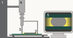
The main system elements are inspection stand, light source, optical system, image recorder, image processor and display (figure 1). The performance of an inspection system regarding the fault detection rate, user friendliness and flexibility is basically determined by the interaction of these elements.
Complete inspection of a component requires moving along such a ball-grid array and viewing the different rows of solder balls. With dimensions of 50µm at the component, this movement must have the appropriate precision. Needless to say, the object to be inspected on the board must first be physically accessible with the optical system. Fast adjustment of the table, coupled with fine adjustment is a good way to meet both requirements.
BGAs represent one area of application. The inspection system will be all the more useful, however, the more varied the possible applications are. Verifying solder joints in general, seeing the inside of different connectors, inspecting plated-through holes and inner solder meniscuses constitute an incredible variety of applications and require mechanically easy adjustment of the optical system. Turning and tilting the optical system should therefore be an essential feature of the inspection machine.
Flexibility is usually possible only through modularity. Exchanging the optical system or the camera and attaching filters or optical elements such as converters are all features that may be necessary for adapting the system to particular application requirements. For example, the inspection camera can be used to turn a triocular microscope into a video microscope, or the BGA optical system can be replaced by a top-viewing optical system, or a two-fold converter can be introduced in the system. Final- ly, easy exchangeability is important for service.
The core of the system
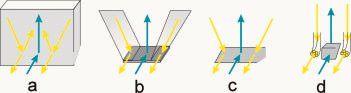
The fundamental task of the inspection system is to produce an instructive image in a gap with a standoff height of 500µm or less. For this purpose, the inspection head needs a light or image-bending optical element. This bending piece (figure 2) is usually a prism or mirror attached to the head end of the optical system.
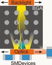
Since components on a PCB are being packed more and more closely together, the inspection head must be as small as possible. Figure 3 shows a schematic of a BGA with the optical system directly adjacent. Here the „footprint“ of the optical head is essential. The depth refers to the theoretically minimum distance between other SMDs and the BGA. The width indicates how far the head can move towards the edge of the BGA without bumping into the sides of other components. The farthest row of a BGA should also be accessible. A depth of approximately 1.5mm and width of about 5 to 6mm are standard for the inspection head. (The depth and width are determined at a height of about 1mm, the approximate height of most SMDs).
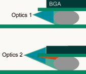
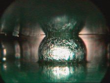
While mechanically the minimum dimensions are clear, optically they are not at all. If the user wants to verify all solder balls under a BGA, then the optical system must provide sharp images from front to back; that is, it must be focused through the depth of a BGA. Figure 4 shows two optical systems (dark-blue color indicates the area that cannot be focused). Optical system 1 (top) is therefore well positioned at the BGA. Even if it were possible, moving the optical system closer to the BGA would bring no benefit, since the system would not deliver a sharp image of the solder ball. A greater distance from the BGA is not problematic. It would not affect the focus and would even remedy another difficulty: if the optical cone does not have an ideal height that is less than the gap or standoff height of the BGA, then the upper joint of the solder ball cannot be viewed, as shown by the red area (figure 4 bottom). It’s easy to see, however, that even at a greater distance, the optical system would flatten the angle to the solder ball and reduce the non-viewable (red) area. Increasing distance improves the image quality. Since maneuvering space around a BGA is often not available, an excellent inspection head proves its merit with good images even when placed directly against the BGA.
Image recording needs light
In order to see or visualize an object, light is essential. What is physically possible must serve the inspection goals, for obtaining optimal results. However, there are ”physically impossible” conditions: a ball covered by another ball cannot be optically viewed, and the lower a ball lies under the BGA, the less light this ball receives (figure 3). Despite this problem, the inspection system must be able to supply information for assessing the solder-joint properties: the surface structures of the balls, connection to the landing areas, characteris- tics of meniscuses, meniscus form, bridges, presence of solder balls, flux residues and other anomalies.
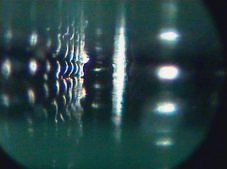
To fulfill these criteria as much as possible, a combination of frontal light and backlight has established itself as the ideal illumination. The frontal light illuminates the outer balls and enables excellent assessment of the surface structure, the joints, the meniscuses and the detection of certain faults, such as micro cracks. Slanting the optical system at an angle to the BGA edge often allows the same evaluation for the nearest, inside rows. The backlight illuminates the ball from behind. The edges and therefore the form of the outer ball (marked „a“ in figure 3) become more clearly recognizable. The image shows more contrast (figure 6). The benefits of backlighting become most evident when the inspection head is used to view between two rows of balls (see figure 3). The backlight immediately indicates whether solder bridges exist and whether the passage is free of any residue. If the optical system has a wide focus range, then its possible to focus row after row and detect the outline of the inside ball by backlighting. An example for this: light path to the inside ball (marked „i“ in figure 3; figure 5). This way, the form, meniscus and various anomalies can then be evaluated.
If a user needs to view all rows of a BGA successively, then he has to move the inspection optical head. As figure 3 shows, practically only the light incident directly opposite the backlight contributes to the inspection of the inside solder balls. The intermediate balls block light coming from the sides. A controllable method for ensuring constant good illumination under the BGA can therefore only lie in guiding the backlight with the inspection head. Coupling within a single system is appropriate in this case.
Image quality and system properties
The image quality is determined by the individual properties of the system elements. These elements are: the inspection head, the design of the optical system for focusing to the middle of the component, the image details and resolution, and adequate and spatially optimized light intensity. Also, the adaptive optical system of the camera, the camera itself with its image sensor, the resolution of the video monitor or, alternatively, the frame grabber and the VGA monitors equally affect the image quality. In other words, what eventually is of high interest for users is the system resolution. With the image, what’s important is how large the smallest structure on the object must be in order to be visible.
Not essential is that the camera has a correspondingly high resolution, for example – even if such a number is easily determinable and therefore comparable. Rather, the weakest member in the chain of optical elements determines the quality of the displayed image. Therefore, low quality of an optical system cannot be compensated by better camera quality. The simplest test for determining the system quality is to inspect a structure and to view the display of this. Such a structure can be a defined reticule plate. The issue is then how many line pairs can be seen on the monitor.
Here it must be noted that the number of lines decreases as the light conditions become poorer. The image details must also be considered. For example, if two complete balls are to be viewed on a BGA with a grid of 1.27mm, then the image area is 2.54mm. If the attained resolution is 288 line pairs, then structures are still visible along the horizontal direction of size 2.54mm divided by 288, or barely 9µm. If another optical system allows precise viewing of a ball (1.27mm) and if a resolution of 200 line pairs can be attained, then structures of about 6µm are still seen, i.e. considerably smaller. Of course, the user will then also have different image details. Image details should be considered good if the structure in question is completely visible. That is, on a BGA the ball should be completely recognizable with its lower and its upper joints (figure 4/optical system 1; figure 6).
Suitability on the shop floor
Visual BGA inspection systems should always be compatible to ESD requirements (especially CMOS devices on a board assembly are an issue). There are multilayer-board assemblies which represent values close to the price of an inspection system. Protection of such costly assemblies should therefore have priority. Simple, sturdy and easily understandable control functions are another must-have.
The suitability of the inspection head for use in a production environment depends on the protection against accidental damage. Some inspection systems require direct contact of the unprotected optical head or glass mirror with the board. The attached prism or mirror edge of such an optical head can be easily damaged, which generally leads to image loss and expensive replacement or repair. The problem is not solved by an apparently convenient exchange of the head.
The optimal solution lies rather in integrated and sturdy prism protection. The version shown in figure 2d can of course be more easily protected than that shown in 2c, for example, since the contact surface on the assembly in figure 2c is clearly larger, and the attachment of protective mechanisms would be considerably more difficult and more space-consuming. Well-protected heads have the advantage of „near-zero“ damage: no risk of breakage when handled properly. Moreover, since the bottom edge cannot become „frayed“ by damage, the optical pupil can be placed very far down. This is very advantageous particularly with the sort of flat columns encountered in CSPs or flip chip devices.
Costs versus benefits
The investment in a system is offset by the possible benefits of that system: precise fault detection and related savings potential in the process, so that the investment quickly pays off; applicable beyond mere BGA inspection (high flexibility); cost of ownership and service life. An inspection system is economical only if it reveals all real-life defects. If a system needs software as a supplement to assist users in the analysis and evaluation of results, then the reaction to flaws in the manufacturing process can occur with considerably greater precision.
The prospective buyer’s cost-benefit analysis should also consider the cost of waste in production, and the added value of the knowledge gained by employing the system in research and development. The amortization of an investment can be optimized if such a system can be used more flexibly and is therefore available for other tasks, such as top-view inspections. An estimation of the cost of ownership should also consider the inspection head as a fragile element. The investment in a system with an unprotected inspection head can become a costly venture.
In a nutshell: successful BGA inspection on board assemblies, with the aim of process improvement, presupposes an efficient system. The detailed knowledge of the necessary properties of the individual system elements, coupled with a reliable demonstration performed directly on the inspection objects, forms the realistic basis for deciding on the investment in an inspection system.
ZUSAMMENFASSUNG
In vielen Baugruppenfertigungen finden sich zunehmend visuelle Inspektionssysteme, die man geradezu ideal für die Verfikation von BGA-Lötstellen anwendet. Diese kostengünstigen Lösungen liefern Bilder bei räumlich äußerst beengten Verhältnissen, wobei man mit einem winzigen optischen Kopf unter die Bauelemente in die Lücke zur Leiterplatte fährt. Vor der Investition sollte der Anwender klären, welche Anforderungen solche in die nähere Auswahl gezogenen Systeme erfüllen können.
RÉSUMÉ
Dans de nombreuses fabrications de modules, on trouve de plus en plus de systèmes d’inspection visuels que l’on emploie de façon pratiquement idéale pour la vérification des joints brasés BGA. Ces solutions économiques livrent des images dans des espaces extrêmement étroits en guidant une minuscule tête optique sous les éléments dans l’interstice menant à la plaquette. Avant de se décider pour l’investissement, l’utilisateur devrait s’informer quelles exigences les systèmes sélectionnés peuvent remplir.
SOMMARIO
I molte produzioni di gruppi costruttivi troviamo sempre più spesso sistemi visuali d’ispezione, che vengono impiegati proprio per la verifica di punti di saldatura BGA. Queste soluzioni economiche forniscono immagini in condizioni di spazio particolarmente ristrette, traslando una piccolissima testina ottica sotto gli elementi costruttivi nella fessura del circuito stampato. Prima dell’investimento l’utente dovrebbe comunque chiarire a quali rivendicazioni dovrebbero corrispondere queste soluzioni nell’ambito di una scelta dettagliata dei sistemi presi in considerazione.
Share:


