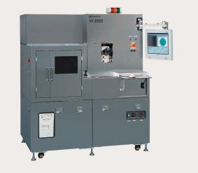
Topcon (represented in Europe by Macrotron Process Technologies) introduces its Vi-series, a universally applicable high-res inspection system which is suitable for automated microscopic defect detection and inner dimension measurement of all wafer sizes from 2 to 8-in, framed wafers and chips in trays. With inspection of inner die object dimensions as well as locations and angles between objects, it is especially suitedfor final IC inspection, MEMS and discrete applications. This instrument detects particles, chippings, pads, ink dots, film defects, etc. from mm-size down to submicron with high reliability. Auto alignment adapts to each displaced chip after wafer sawing/ expansion. Reportedly, ev-en high brightness and contrast ranges of images won’t negatively influence the detection sensitivity. The parameters are individually adjustable for many areas within one field of view. In combination with the optimized Min-Max algorithm, providing a quarter of a pixel resolution, even complicated area inspections are accomplished at high defect recognition rate and a repeatability of >98%. The viewing area can be adapted to die size and keep the adjusted sensitivity at optimum through-put, achieving 52 wafers/hr. Import and export of defect maps to all common probers and pick& place systems, off-line programming, review and inking function are offered optionally. Data can be transferred to the host in SECS/ GEM format.
Semicon Hall A1/booth 402
Share:


