One of the often overlooked but very important assembly steps in packaging is the die bonding process. With the increased use of dies that require extremely tight tolerances in their placement, special care should be taken by advanced die-bonding equipment. Z-positional bonding might provide an answer to this challenge.
Jürgen Seibert, Datacon Semiconductor Equipment
Mainly consumer electronics determines the way manufacturing technology is evolving. Consumer demand for personalized electronics devices, very often featuring wireless functions, has enabled the growing convergence between three traditionally different markets or product groups, respectively: traditional consumer electronics, communication devices and computer technology. This demand has been made possible by the ongoing advances in miniaturization and communication technologies. The trend towards ever smaller and faster electronic endproducts that are increasingly multifunctional and yet get cheaper and cheaper, is affecting the whole electronics food chain, including the semiconductor-backend with assembly and test.
Challenging theassembly side
Impressive downscaling of transistor structures has resulted in ever more shrunken dies with millions of gates on a square centimeter. Currently commercially available microprocessors are just touching the 3GHz operating frequency, and doubtlessly this will very soon go even higher in the gigacycle range. Naturally, devise package design and assembly technologies need to keep-up with this rapid evolution. Moreover, the continued integration of complete systems-on-a-chip or systems-in-a-package puts requirements that are even more stringent on the type of package to be used, depending on the application envisaged. A major driver of technology today is the increased need for miniaturized, handheld wireless communication electronic appliances.
The higher complexity of circuit designs and device densities for these applications require more and more tests to detect possible flaws or defects in design and manufacturing. The reason for this is that defect levels are becoming increasingly more critical for manufacturing. All these factors have changed the nature of backend assembly and test into a very critical part of manufacturing in the electronic components industry.
At the business side of the story, integrated device manufacturers (IDMs) need to introduce their products on the market place faster than ever (shorter time-to-market). On the whole electronics food chain, this reflects on to the users of endproducts encompassing those ICs. Chip manufacturers are faced with ever faster time-to-market or time-to-volume, and need to deliver in faster turnaround cycles. The same is true for backend-assembly houses (foundries). These third-party assembly subcontractors are a fast growing phenomenon. The reasons for the rise are the same as for the flourishing wafer-fab foundries: reductions of capital/investment risk and overall cost, and the opportunities they provide for IDMs to focus on activities in their core competences. Third-party subcontractors are now among the most advanced manufacturers, both for chip production as for backend assembly and test.
In turn, this increasingly introduces a number of challenges to equipment suppliers, to match exactly the requirements technically and for cost-of-ownership. With subcontractors, in order to deliver a large variety of packaging solutions, the equipment they need must be designed to be highly flexible, yet providing very high throughput. In addition, more and more of their clients require that custom-made solutions be offered by the backend subcontractors at very short cycle times. In short, production equipment should be fast, highly reliable, offer a variety of the latest technology features, be easily adaptable to different standards and assembly techniques and yet cost-effective. This is really quite a severe challenge for backend-assembly equipment suppliers.
Accuracy tradeoff versus throughput
One of the process steps in the assembly of dies is the attachment or bonding of a die on the substrate (see figure 1). With die attach, different technologies can be identified, such as face-up wire bonding, tape automated bonding or flip-chip technology. In the traditional definition, die attach includes the picking, alignment and placement of dies on a substrate. Different chip-attach placement techniques might be employed in a multi-chip module. Multiple die-bonding machines will increasingly find their way to the market. In view of this discussion, some important questions arise: how fast can a die be aligned and affixed? – And will die bonding become a major bottleneck in the evolution towards ever more complex packages?
The answers to these questions aren’t easy ones. Placement accuracy refers to the X, Y, and Z-directions and the tilting angle theta. As placement accuracy is proportional to the time needed to perform the attachment step (i.e. its speed), more constraints on accuracy will affect the throughput of die-bonding equipment. In some cases, special care is required regarding the die-bonding step. High frequency GaAs die-attach applications are one example for that. Another is the increasing use of CSPs. So, where should the trade-off be placed: accuracy versus throughput or vice versa?
The growing application of chip-scale packaging (CSP) poses real challenges in this matter. CSP technology refers to a die encapsulation (i.e. packaging) that is no more than 20% larger than the chip itself. Perhaps the biggest issue in CSP die-attach is its small size. The smaller the footprint, the greater the accuracy should be in the placement step. Its small footprint requires special care in assembly, not in the least in the die-attach step of the process. For the assembly of CSPs, many different technologies are very often used, including leadframe substrates with the active side of the die faced up. Alternatively, the active surface can be faced down, using an elastomer or PCB material, a leadframe, flex or a simple adhesive layer. Many assembly tools cannot invert the die before mounting. This renders visual inspection by operators impossible. The placement tool, using vision and pattern recognition systems preferably in one and the same unit, should therefore do any correction of the orientation during placement. In turn, this might affect throughput considerably. Increased resolution requirements increase the need for stepping motors in movement for placement and for inspection to be more accurate and, therefore, often slower.
Controlling the bond-line thickness
The bond-line thickness (BLT) is the distance between the bottom side of a bonded die and the top side of the substrate. The larger these variations, the more difficult to obtain die placement with high accuracy. More and more extremely tight BLT tolerances and die-tilt tolerances are normal in assembly. The worst case would be that most of these applications have to be carried out on BGA (ball-grid array) strips with considerable local and global warpage and thickness variations. Dimensional tolerances of BGA substrates can amount to up to ten times compared to traditional metal leadframes.
Apart from the substrate, die-thickness variations must be taken into account as well. This includes within wafer differences as well as from wafer to wafer. The variation within a single wafer can be ±1mil or more, while discrepancy from wafer to wafer can amount to up to ±1mil or more.
Z-positional bonding
The tight tolerances mandatory for die placement at high enough accuracy at extreme conditions such as for high-frequency GaAs-die or CSPs, requires die-attach equipment that takes care of these conditions. At Datacon, with Z-positional bonding, a novel method was developed that determines the substrate warpage/thickness and die thickness of the selected bond site. This is carried out while the die is held on the tool.
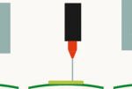
In this process, a die is picked from a wafer or other carriers such as a waffle pack or Gel-Pack with the bond head. While the die is held, the bond head moves down until the die touches the top surface of the substrate. This determines the zero Z-position, relative to the desired bond site. The bond head moves back-up and dispenses epoxy on the bond pad via the dispensing system. The dispensing height is automatically adjusted using the Z-information from the previous touchdown. Once the epoxy is dispensed, the bond head places the die on the substrate to theprogrammed Z-position and BLT. This method results in a much better BLT consistency and yet does not add much delay time to the bond cycle.
With Z-positional bonding, there are two possible applications: placing dies relative to the actual substrate height (figure 3). Here the die is picked-up as usual, but with the Z-positional tool. The bond head moves to the desired bond position and then downwards until the die touches the surface of the substrate. This determines zero Z-height position (step 1). With this process step, the system eliminates the influence of die thickness and substrate height variations on the resulting BLT. The die is then lifted again and the dispenser applies epoxy on the bond pad (step 2). The following final bonding process (step 3) is carried out. For this step, the tool knows from the zero reference Z-height determined in step 1 what travel distance is necessary to achieve the desired BLT.
An outlook
Die bonding is perhaps one the biggest challenges in the assembly process of small, complex packages that necessitate extremely tight tolerances, both in thickness variations of die and substrate as in tilt tolerances. New and highly flexible die-attach equipment, capable of placing dies at high accuracy combined with high throughput, are necessary for the backend-assembly industry. Hopefully, it will prevent bottlenecks on the road towards the rise of highend-assembly process technologies.
ZUSAMMENFASSUNG
Das in der Halbleiterfertigung oder auch bei der direkten Verarbeitung von ungehäusten Chips auf Boards nötige Die-Attach wird bei den fortlaufend weiter reduzierten Plazier-Toleranzen zunehmend zum Flaschenhals in der Fertigung. Dabei steigen durch die Miniaturisierung sämtlicher Geometrien zunehmend die Anforderungen. Mit Z-Position-Bonding hat Datacon ein Verfahren entwickelt, das sich als Lösung anbietet. Dabei werden während des Die-Attach die Toleranzen von Substrat sowie Bond-Fläche erfasst und dann im Plazierprozess’ im Interesse hoher Genauigkeit gezielt ausgeglichen.
Share:
