


Field-array packages such as ball grid array, chip scale and flip chip combined with the trend to Pb-free manufacturing are creating challenges. The question is how to confirm quality and reliability, even if there is no direct electrical or visual access to device terminations on a board? A non-destructive method, for example X-ray systems providing 2D, 3D and tomosynthesis imaging, can be a valuable tool to analyze solder print or joints and assemblies in order to catch data on product quality.
Alf Björklöf, reliability manager, Tellabs Oy, Espoo, Finland
The major problems are that the solder joints are quite often hidden, and lead-free solder surface is dull or grainy. Traditionally, the criterion for a perfect solder joint has been a shiny surface with small wetting angles. Unfortunately, a shiny surface might hide many clues for a poor soldering process. Destructive tests, like micro-sectioning or thermally accelerated cycling tests, will also reveal these defects. But these methods are time consuming and will destroy the samples.
The Finnish Company Tellabs installed an 2D/3D X-ray system, Feinfocus Visualizer, for analytical studies in the group’s reliability systems laboratory. The application focused on Pb-free soldering process evaluation, manufacturing and repair process improvement, as well as defect and component-related analysis. The interpretation of the X-ray images could have been difficult without the groups‘ extensive experience in electronics manufacturing and packaging in combination with knowledge in basic sciences. The experience gained so far has proven the value of the versatile X-ray system for supporting R&D, component engineers as well as manufacturing to supply reliable products.
Theory at a glance
The operating theory of an X-ray system is basically simple. The higher the accelerating voltage in the tube, the harder the radiation. It features high radiant emission and a short peak wavelength of electromagnetic energy from a target, allowing higher penetration into the material. The radiation from the target forms a cone. The geometrical distances of target and sample to the image intensifier determine the magnification factor. The practical magnification range is 2 to 50 (maximum 1.5 to 60). A three-dimensional sample projected on the flat surface of the image intensifier will distort the image slightly by shadowing the edges and projecting the items outside the center of the cone as demonstrated in figure 1.
The X-ray absorption in different materials is proportional to the thickness and density of these materials. Metals like tin, indium, nickel, copper, bismuth, silver and lead are slightly deviating from this density principle. Anyway, it is important to have an idea of how thick and what material the object is under study. Plastic materials in packages and boards as well as reinforcement materials like glass fiber or quartz and alumina fillers will absorb the radiation, thus smudging the images. These factors will affect on the voltage and current settings on the X-ray system to a-chieve a clear image of the sample. A good practice is to start with low settings and increase them for best resolution.
The following examples are merely brief studies, just to give an idea of what an X-ray system can do. In the reliability laboratory we also have other equipment, which is used to compare or verify the results obtained by X-ray inspection.
Open solder joints
A 2D image might not give all the information needed to interpret the sample correctly, despite the possibility to inspect under different angles. The Visualizer works on the principle of making digitized 2D images by taking a desired number of projections and beam angles. The table with the sample and the image amplifier are moving synchronously while the tube is fixed. The acquired information can then be mathe-matically processed using the image pixels and vectors to form slice images (tomosynthesis). This allows the sample to be studied layer by layer, looking at the slice images to detect e.g. open solder joints.
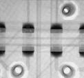
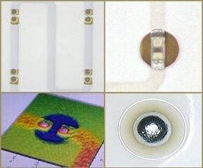
For example, a failing PC motherboard was studied to find the reason for malfunctioning after adding an interface module into an edge connector. Close to the connector on the bottom side of the motherboard, a PBGA-256 was soldered, featuring a 1.27mm ball pitch. The corner solder joint was suspected to have been broken due to board warping during the insertion of the daughterboard. The 2D inspection did not reveal anything abnormal. Then the area of interest was defined to have 1mm height, and 200 slices were formed. The slice images revealed an open joint not in the corner but in the second column and third row of the connector (figure 2).
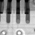
Voids in solder joints
The pixels in each slice layer are recombined to voxels (3D pixel), thus forming 3D images. The acceptance criteria for voids in solder joints have been discussed many times and are still under consideration. The size of the void is not as important as the location of it. If the void is close to the solder pad on the board or the component, it is a poor solder joint in respect to solder wetting or tensile strength of the joint. The creep fatigue will break the solder joint in an early stage of operational lifetime.
A 3D image gives very detailed information about the void location, size and shape (figure 3). The image or a selected portion of it can be „micro-sectioned“ on the screen and turned in any direction for analysis, which is demonstrated in the image series (figure 4). This sample is a PLCC socket with obvious voiding and solder wetting problems.
Analysis on package and board
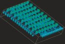
Package types can be analyzed non-destructively to understand the implications on reflow soldering profiles. These materials willbe be studied rough-ly based on the rela-tive radiation absorption and object thickness. The device interconnections can also be studied. For example, a ceramic BGA package was analyzed, formed by a double-sided ceramic substrate with 1mm pitch solder balls on the bottom side. The substrate also contains solder-filled via holes and thermal vias. The die is flip-chip-style mounted to thickfilm conductors and protected with a plastic lid glued to the base (figures 5). Here, the area of interest has been cropped in the X-ray system, and images can be magnified.
Despite the large differences in the material thickness in the samples, the 3D reconstruction method can display various details in electronic assemblies (figure 6). Possible applications can be in the area of income inspection, failure analysis, design verification, etc.
Process monitoringis a key issue
In SMT soldering, 2/3 of the production-based failures are caused by improper paste printing. Therefore, it is essential to monitor this process, and this is also the most cost-efficient method of controlling and adjusting production quality. The source of process-related defetcs can be corrected immediately, and misprinted PCBs can be cleaned and reused in order to reduce costs. An X-ray control of the solder joints after reflow will also detect the defects, but monitoring and rework costs are significantly higher than with the control right after paste printing. Therefore, it is mandatory to know a production process in details, and then to decide where and how to monitor for optimum performance and efficiency.
It is unlikely that just a single inspection machine or tester can provide all the information needed to control, correct and support the manufacturing process in all details to achieve high quality and reliability for a board assembly in every production stage. Paste print monitoring, pre-solder automated optical inspection, in-circuit or functional test and in-line or off-line X-ray inspection definitely do not exclude each other. Depending on the product category and manufacturing process, a process monitoring system has to be defined in order to provide the optimum in investment, production, warranty conditions and repair costs.
Share:


