Without doubt, the International Technology Roadmap for Semiconductors (ITRS) is one of the great achievements of the electronics industry. It forces a worldwide, forward looking consensus on how the chip industry and its tool and materials suppliers proceed to keep the fast-paced march of innovation going to the self-imposed drumbeat of Moore’s Law.
However, the constraints of physically downscaling the Si-CMOS process, which traditionally has been its centerpiece, get harder to overcome with every new bi-yearly edition of the ITRS. This year, with a full revision due after the 2004 update, major changes will occur in the final document to be released later this year. In the run-up to the 2005 roadmap, Semicon Europa, held in Munich, added a public ITRS conference instead of the usual closed-door meetings to its schedule. This marks a strategy change as the roadmapping issues are getting harder to deal with – the red boxes marking no known solutions are in some instances just one to two years away.
Thus, the roadmap clearly reflects the challenges ahead if the three-year generational chip progress (a slight slowdown from the recent two-year advance) is to be extended to the future. As a consequence, new chapters and topics have been added, and roadmapping is focusing not just on general manufacturing issues but also on real products and architectures of future product categories. Consumer products are now driving the entire supply chain of the chip industry – in terms of its technology but even more so in terms of setting ever lower price points for its ever more complex deliverables.
Therefore, the Munich ITRS conference took pains to add “emerging research devices and materials” to its timeline. The other urgent topics, Semi notes, are design and system drivers, test and test equipment, process integration, lithography, modeling and simulation, front-end processes, interconnect, assembly and packaging, metrology, yield enhancement and factory integration. 15 such topics and a like number of international working groups, busying nearly 1000 contributing industry experts in the five major chipmaking regions USA, Japan, Korea, Taiwan and Europe.
What are the challenges in the view of the ITRS working groups? On the front-end, it’s clearly EUV (extreme ultraviolet lithography), as Paolo Gargini of Intel, freely admits. It will take an “aggressive push”, he says, to get EUV on-stream in the timeline of downscaling to the 45nm half-pitch. “Control of critical dimensions” is the main problem here.
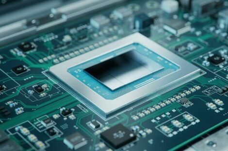
As mainstream wafer technology has entered the 90nm realm, the traditional dimensional scaling of Si-CMOS must be complemented by charge-carrier mobility enhancement techniques (strained Si) and low-k dielectrics. Green materials (Pb- and halogen-free) make their inroads; organic semiconductors are on the horizon (as carried out and funded by European research institutions). In any case, says Wolfgang Arden of Infineon, “the 2007 deadline for 65 nm will be met, for sure – despite a number of challenges”.
Sure enough, there are plenty of challenges – not the least of them stemming from demands in assembly and packaging. Thus, says Mart Graef of Philips, “in the 2005 ITRS, packaging issues are extended”. Besides packaging getting more play, there are also MEMS and optoelectronics included in the proper roadmapping process.
In focusing on assembly and packaging, the 2005 ITRS notes that “packaging has become the limiting element in systems cost and performance”. Why? Because consumer devices, driving more than half of worldwide chip revenue, command the next stage of functionality at a very dense packaging level. In time, consumer devices will force the transition to biochips and organic semiconductors made of printable circuits.
So, in terms of packaging, the path to multi-level (3D) system integration is mapped out, with active and passive components coming embedded in separate PCB layers, or with embedded optics, structured as stacks or partitioned in subsystem packages. All this, says Bill Bottoms, speaking for the ITRS assembly and packaging work group, will be explicitly addressed.
Among the near-term (>45nm, up to 2010) challenges are: embedded components, improved organic substrates, design tools and simulation of co-designing chips, packages and substrates, the impact of Cu/low-k and high-current-density packages which suffer at small dimensions from electro-migration. In the longer term (<45nm, after 2010), there is the heightened problem of sufficient economic margins in packaging, because packaging cost reduction won’t follow die outlay reduction induced by the larger (450mm) wafer. Another challenge is realizing high-frequency functionality at 20 lines/mm density on the substrate. Then there are the uncharted waters of organic and bio-devices – all of them requiring other packaging and assembly technologies.
The task of designing and processing adequate solutions for this certainly doesn’t get easier – as will be reflected in the ITRS assembly and packaging chapter. Among the issues to be covered here are: electrical crosstalk and power distribution at a very small dimensional scale. Next: thermal dissipation and mechanical stress need to be addressed in a co-design approach and covered by an extra roadmap based on chip size. Also, next-level chip interconnect needs to be dealt with through flexible connections, especially with thinned wafers placed in flexible modules.
A last word on factory integration, from reticle and wafer processing to final product assembly: key words are cost, productivity and speed – all in their own realms of desirable or tolerable dimensions. Process planning for 450mm wafers (due by 2012) has already begun, and EUV is anticipated for 2013. All these issues pose major hurdles. In the short term, the efforts of factory integration will continue centering on increased fab complexity and scalability, besides meeting next environmental restrictions on materials and waste. In the long term, however, other structures need to be integrated in the production flow. The industry will have to measure up to a new paradigm of post-conventional chip and packaging technologies, causing it to change and renew itself – again.
Werner Schulz
EPP EUROPE 400
Share: